Gallium-nitride-on-diamond wafers and manufacturing equipment and methods of manufacture

a technology of diamond wafers and gallium nitride, which is applied in the direction of crystal growth process, polycrystalline material growth, chemically reactive gas growth, etc., can solve the problems of reducing cooling requirements, limiting the performance of algan electronic and optoelectronic devices, and the most pronounced deficiency of algan/gan hemts, etc., to achieve the effect of improving the thermal performance of algan/gan hemts

Active Publication Date: 2016-06-07
AKASH SYST INC
View PDF18 Cites 17 Cited by
  • Summary
  • Abstract
  • Description
  • Claims
  • Application Information

AI Technical Summary

Problems solved by technology

In spite of the high-temperature performance (owing to its wide bandgap and high critical field), GaN electronic and optoelectronic devices are limited in performance due to relatively low thermal resistance of the substrates commonly used for growth of GaN.
This deficiency is most pronounced in high-power microwave and millimeter-wave transistors and amplifiers where reduced cooling requirements and longer device life, both benefiting from lower junction temperature, are in critical demand.
From the point of thermal management, the presence of the nucleation layer 2 (part of the transition layer) is detrimental to device thermal performance.
Namely, due to multiple layer-boundaries within the transition layer, alloy scattering, and dislocations, the transition layer generally presents a significant barrier to heat flow perpendicular to the layers and thereby limits the device thermal conductance.
Finally, materials used commercially for the substrate 1 have low thermal resistance further contributing to the overall low thermal resistance of the devices (eg. sapphire, silicon).
The result of these materials and structure limitations is that conventional AlGaN / GaN field-effect transistors are limited thermally, but could be made better if its the thermal resistance could be somehow reduced.

Method used


Image

  • Gallium-nitride-on-diamond wafers and manufacturing equipment and methods of manufacture
  • Gallium-nitride-on-diamond wafers and manufacturing equipment and methods of manufacture
  • Gallium-nitride-on-diamond wafers and manufacturing equipment and methods of manufacture

Examples


Embodiment Construction

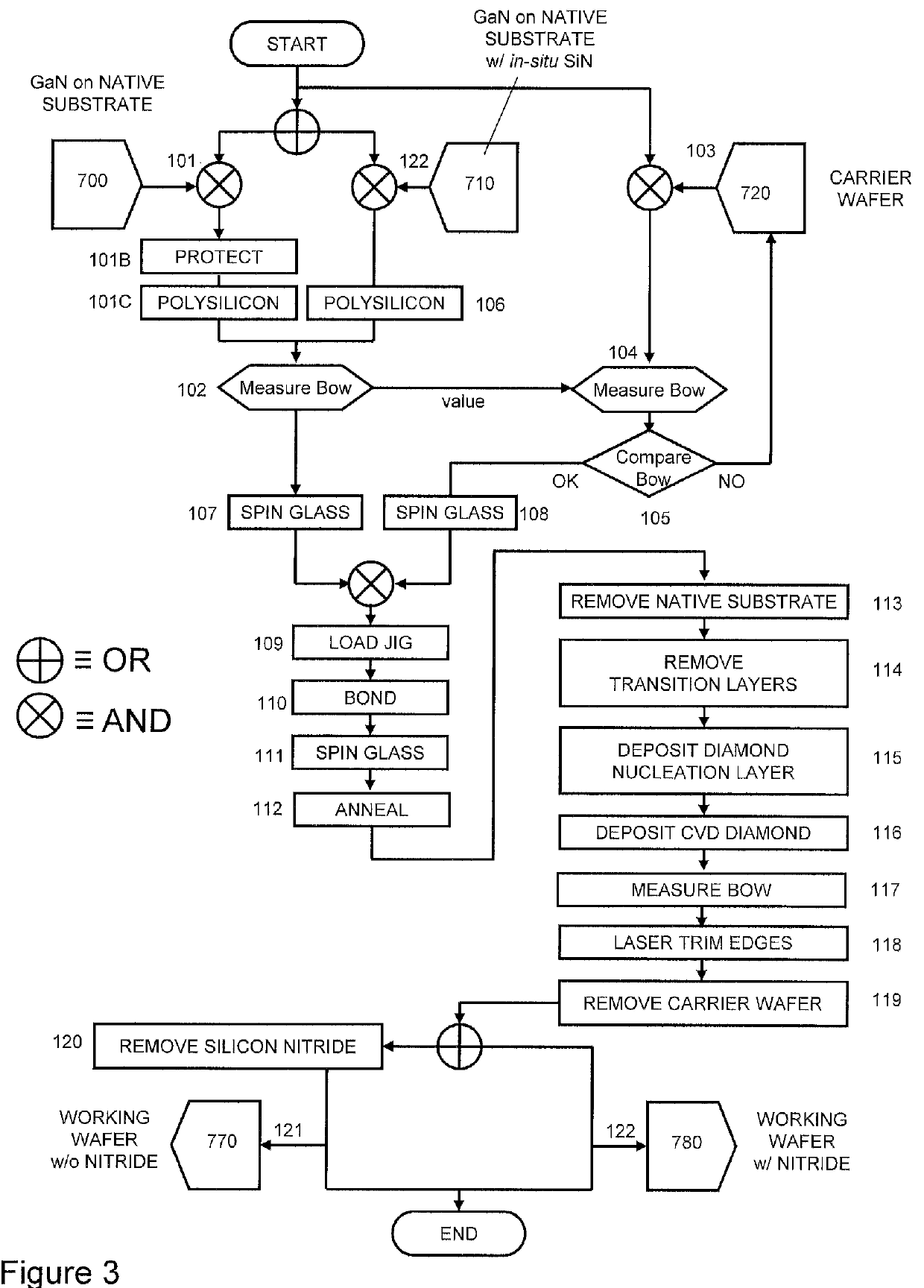
[0052]Preferred methods 100 and 200 are explained with the help of a block diagram in FIG. 3 and other figures that are used to clarify the structure of wafers used or produced by the preferred processes. In Method 100, the wafers provided are “GaN on NATIVE SUBSTRATE”700 having structure illustratively shown in FIG. 4A and “CARRIER WAFER”720 having structure illustratively shown in FIG. 4B. In Method 200, the wafers provided are “GaN on NATIVE SUBSTRATE with in-situ silicon nitride”710 having structure illustratively shown in FIG. 12 and “CARRIER WAFER”720 having structure illustratively shown in FIG. 4B. The methods merge before step 102 and continue with the same steps for either method. Either method can be used to produce an engineered GaN-on-diamond wafer with silicon nitride coating 780 (“WORKING WAFER w / NITRIDE”). Either method can be used to produce an engineered GaN-on-diamond wafer without silicon nitride coating 770 (“WORKING WAFER w / o NITRIDE”) as illustrated in the flo...


PUM

PropertyMeasurementUnit
thicknessaaaaaaaaaa
melting temperatureaaaaaaaaaa
melting pointsaaaaaaaaaa

Abstract

A method for integrating wide-gap semiconductors, and specifically, gallium nitride epilayers, with synthetic diamond substrates is disclosed. Diamond substrates are created by depositing synthetic diamond onto a nucleating layer deposited or formed on a layered structure that comprises at least one layer of gallium nitride. Methods for manufacturing GaN-on-diamond wafers with low bow and high crystalline quality are disclosed along with preferred choices for manufacturing GaN-on-diamond wafers and chips tailored to specific applications.

Description

RELATED APPLICATIONS[0001]This application claims priority to U.S. Provisional Patent Application Ser. No. 61 / 604,979 filed Feb. 29, 2012. The disclosure is incorporated herein by reference.FIELD OF THE INVENTION[0002]The present invention relates to high-power electronic and optoelectronic devices and their thermal management, and particularly relates to methods for fabricating devices and structures that include integration of synthetic diamond films and wafers with wide-gap semiconductors, and more particularly with gallium nitride-based electronic and optoelectronic devices; including high-electron mobility transistors, radio-frequency (RF) electronic devices, light-emitting-diodes, and lasers.BACKGROUND OF THE INVENTION[0003]Thermal management in semiconductor devices and circuits is a critical design element in any manufacturable and cost-effective electronic and optoelectronic product, such as light generation and electrical signal amplification. The goal of efficient thermal...

Claims


Application Information

Patent Timeline
Patent Type & Authority Patents(United States)
IPC IPC(8): C30B25/16C30B25/10C30B29/04C30B25/18C30B25/20H01L21/02C23C16/46C23C16/27H01L29/20H01L29/778H01L21/18
CPCC30B25/16C23C16/271C23C16/463C30B25/10C30B25/18C30B25/183C30B25/205C30B29/04H01L21/0245H01L21/0254H01L21/0262H01L21/02381H01L21/02389H01L21/02488H01L21/02527H01L21/02658H01L21/187H01L29/2003H01L29/7786
Inventor FRANCIS, DANIELFAILI, FIROOZMATTHEWS, KRISTOPHERLOWE, FRANK YANTISDIDUCK, QUENTINZAYTSEV, SERGEYEJECKAM, FELIX
Owner AKASH SYST INC
Why Eureka
Try Eureka