High power impulse magnetron sputtering process to achieve a high density high SP3 containing layer

a magnetron sputtering and high density technology, applied in the direction of vacuum evaporation coating, chemical vapor deposition coating, coating, etc., can solve the problems of high aspect ratio etching, limited reduction, and high cos

Active Publication Date: 2017-07-04
APPLIED MATERIALS INC
View PDF9 Cites 17 Cited by
  • Summary
  • Abstract
  • Description
  • Claims
  • Application Information

AI Technical Summary

Problems solved by technology

While in the past such reductions were limited only by the ability to define the structures using photolithography, device geometries having dimensions measured in micrometers (μm) or nanometers (nm) have created new limiting factors, such as the conductivity of the conductive interconnects, the dielectric constant of the insulating material(s) used between the interconnects, etching the small structures or other challenges in 3D NAND or DRAM form processes.
However, current graphitic, Sp2 type or other carbon hardmask compositions are expected to be insufficient as DRAM and NAND continue their scaling down to under ˜10 nm regime.
The high aspect ratio etch issues include clogging, hole-shape distortion, and pattern deformation, top critical dimension blow up, line bending, profile bowing are generally observed in these applications.
Deep contact hole deformation can be related to lower hardmask density and poor thermal conductivity.
Slit pattern deformation or line bending is due to hardmask material lower selectivity and stress.
However, there are a variety of difficulties with the use of hot filament CVD and microwave CVD processes to form nanocrystalline diamond films.
As a result, precursor gases can react with the metal filament leading to metal contamination issues in the final product.
However, microwave CVD requires a high process pressure which can affect the film uniformity.
Moreover, while microwave generated plasma created by microwave CVD hardware has relatively low ion energies, these generated ions can still attack the NCD grain boundary and induce grain structure disorder.

Method used


Image

  • High power impulse magnetron sputtering process to achieve a high density high SP3 containing layer
  • High power impulse magnetron sputtering process to achieve a high density high SP3 containing layer
  • High power impulse magnetron sputtering process to achieve a high density high SP3 containing layer

Examples


Embodiment Construction

[0023]Embodiments disclosed herein generally relate to a nanocrystalline diamond layer formed on a substrate. Nanocrystalline diamond layers formed by the processes described herein generally have a higher mass density, higher etch selectivity, lower stress and excellent thermal conductivity needed for forming integrated circuit (IC) devices having small feature sizes. Embodiments are more clearly described with reference to the figures below.

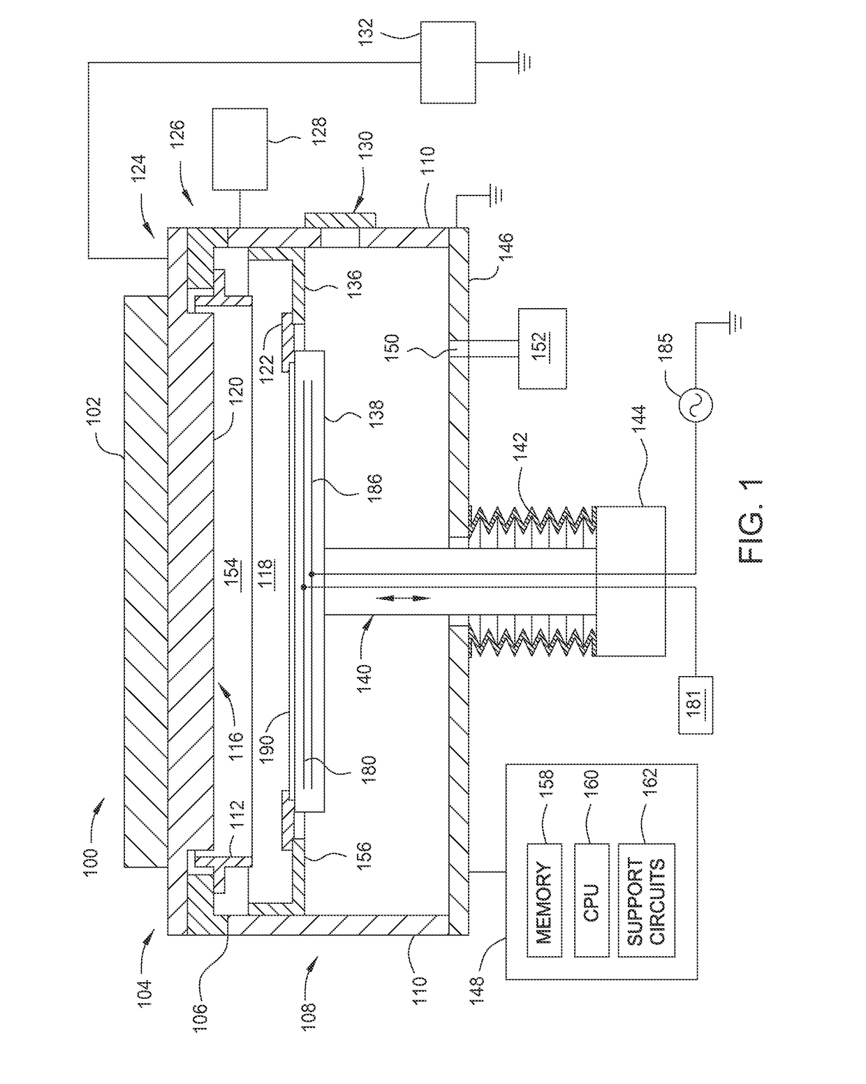
[0024]FIG. 1 illustrates an exemplary physical vapor deposition (PVD) process chamber 100 (e.g., a sputter process chamber) suitable for sputter depositing materials using a high power impulse magnetron sputtering (HIPIMS) process. One example of the process chamber that may be adapted to form the nanocrystalline diamond layer is a PVD process chamber, available from Applied Materials, Inc., located in Santa Clara, Calif. It is contemplated that other sputter process chambers, including those from other manufactures, may be adapted to practice ...


PUM

PropertyMeasurementUnit
temperatureaaaaaaaaaa
pressureaaaaaaaaaa
pressureaaaaaaaaaa

Abstract

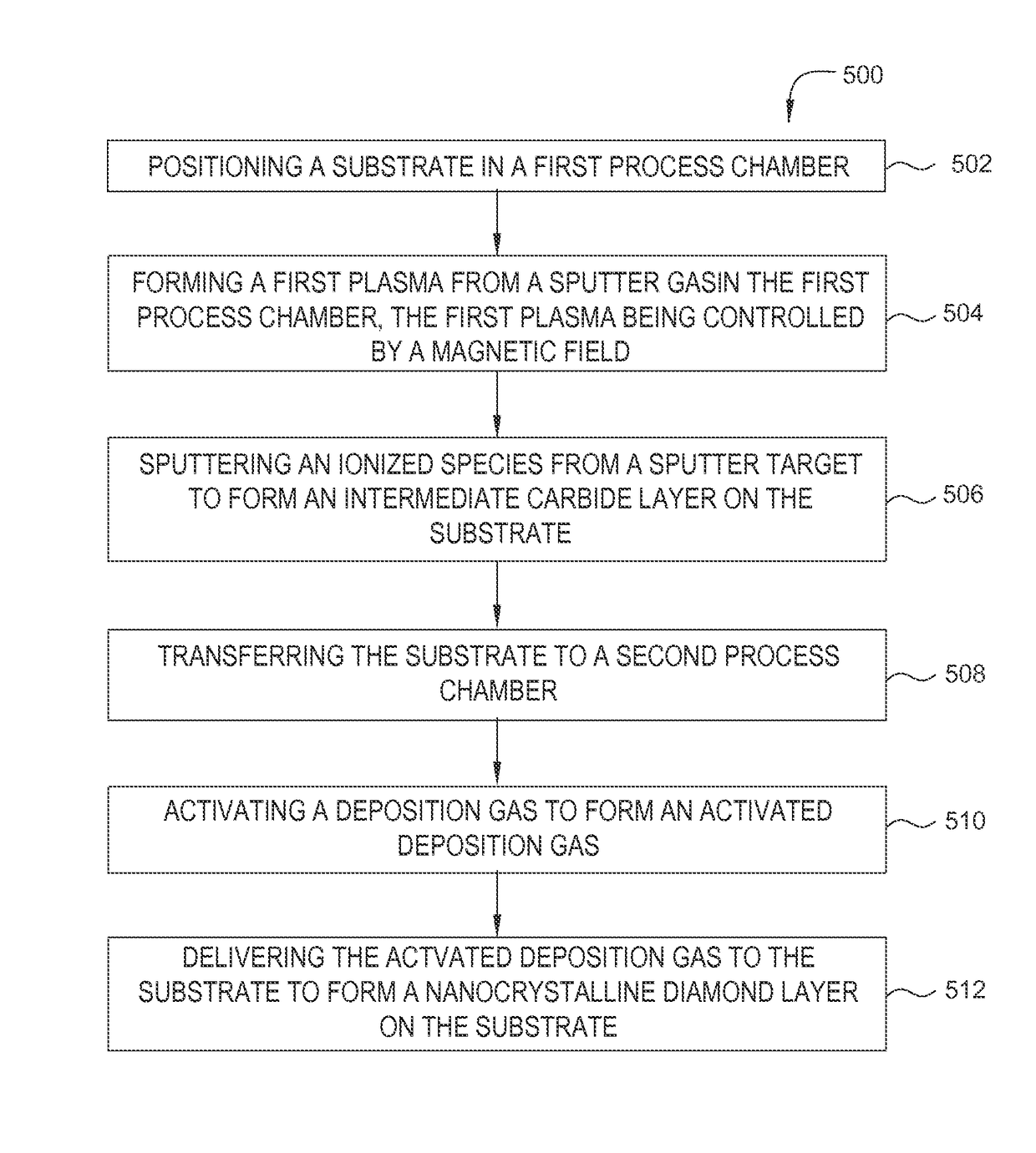
Methods for depositing a nanocrystalline diamond layer are disclosed herein. The method can include delivering a sputter gas to a substrate positioned in a processing region of a first process chamber, the first process chamber having a carbon-containing sputter target, delivering an energy pulse to the sputter gas to create a sputtering plasma, the sputtering plasma having a sputtering duration, the energy pulse having an average power between 1 W / cm2 and 10 W / cm2 and a pulse width which is less than 100 μs and greater than 30 μs, the sputtering plasma being controlled by a magnetic field, the magnetic field being less than 300. Gauss, and delivering the sputtering plasma to the sputter target to form an ionized species, the ionized species forming a crystalline carbon-containing layer on the substrate.

Description

CROSS-REFERENCE TO RELATED APPLICATIONS[0001]This application claims priority to U.S. Provisional Patent Application Ser. No. 62 / 040,809, filed on Aug. 22, 2014, which is incorporated by reference herein.BACKGROUND[0002]Field[0003]Embodiments disclosed herein generally relate to methods for deposition of a film. More specifically, embodiments an apparatus and methods of depositing a nanocrystalline diamond film for use in semiconductor devices.[0004]Description of the Related Art[0005]As the semiconductor industry introduces new generations of integrated circuits (IC's) having higher performance and greater functionality, the density of the elements that form those IC's is increased, while the dimensions, size and spacing between the individual components or elements are reduced. While in the past such reductions were limited only by the ability to define the structures using photolithography, device geometries having dimensions measured in micrometers (μm) or nanometers (nm) have c...

Claims


Application Information

Patent Timeline
Patent Type & Authority Patents(United States)
IPC IPC(8): C23C14/34C23C16/50H01L21/02C23C14/06C23C16/27C23C14/35
CPCH01L21/02266C23C14/35C23C14/0611C23C16/272C23C16/50H01L21/02115H01L21/0262H01L21/02631H01L21/02527H01L21/02595H01L21/02274H01L21/203H01L21/205H01L21/67098
Inventor STOWELL, MICHAEL W.CHEN, YONGMEI
Owner APPLIED MATERIALS INC
Why Eureka
Try Eureka