Catalytic laminate apparatus and method

a technology of catalytic laminate and apparatus, which is applied in the direction of printed circuit aspects, electric connection formation of printed elements, and metal adhesion improvement of insulating substrates, etc., can solve the problems of reducing the fine pitch of traces, destroying the entire circuit board assembly and expensive components, and individual trace layers being laminated together

Active Publication Date: 2017-07-11
CATLAM LLC
View PDF32 Cites 17 Cited by
  • Summary
  • Abstract
  • Description
  • Claims
  • Application Information

AI Technical Summary

Benefits of technology

[0017]In a fourth embodiment of the invention using a conventional non-catalytic pre-preg, a single or multi-layer PCB is formed by a process having a first step of applying a catalytic adhesive to one or both sides of the non-catalytic pre-preg, where the catalytic adhesive includes a resin mixed with catalytic particles and forms a catalytic adhesive layer over the non-catalytic pre-preg. In a second step, the catalytic pre-preg surface layer is selectively partially removed such as by using a plasma cleaning or plasma etching process for a duration of time sufficient to expose the catalytic particles while leaving the underlying adhesive resin which secures the catalytic particles to the non-catalytic pre-preg. In a third step, the partially removed or etched catalytic adhesive is exposed to electroless plating using metal ions in solution which bind to the catalytic particles, which is performed until a substantially continuous conductive layer of metal is deposited. In a fourth step, a pattern mask is applied which provides open areas where traces are desired. In a fifth step, the continuou

Problems solved by technology

One problem of prior art surface mount PCB fabrication and assembly methods is that because the traces are formed on the surface of the dielectric, the adhesion between copper trace and underlying laminate for narrower conductor line widths (known as fine pitch traces) is reduced, causing the fine pitch traces and component pads to separate (lift) during a component replacement operation, ruining the entire circuit board assembly and expensive components on it.
Another problem of fine p

Method used


Image

  • Catalytic laminate apparatus and method
  • Catalytic laminate apparatus and method
  • Catalytic laminate apparatus and method

Examples


Embodiment Construction

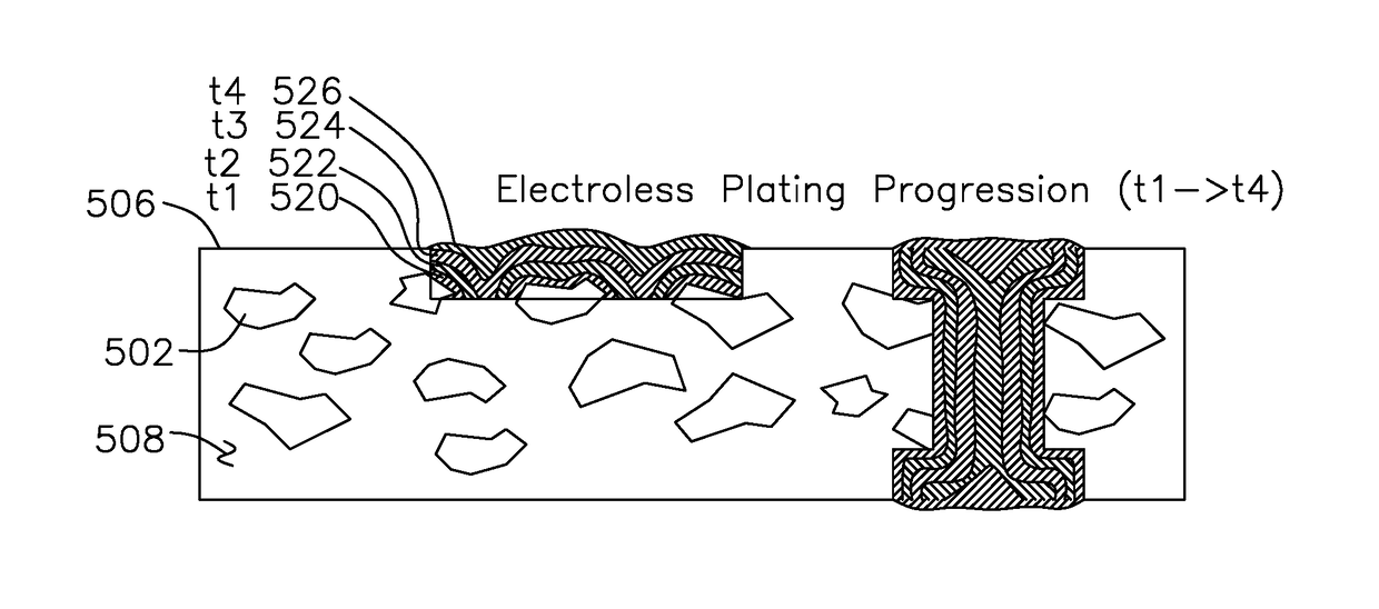
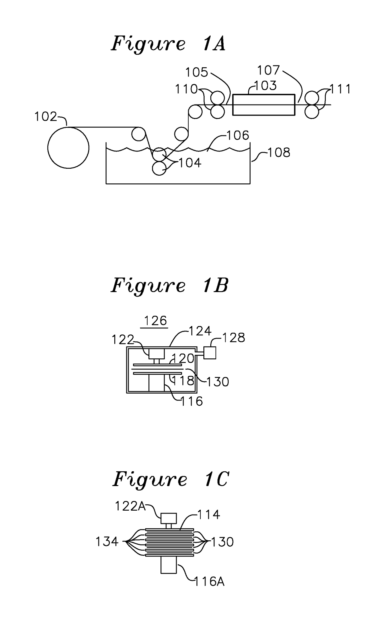
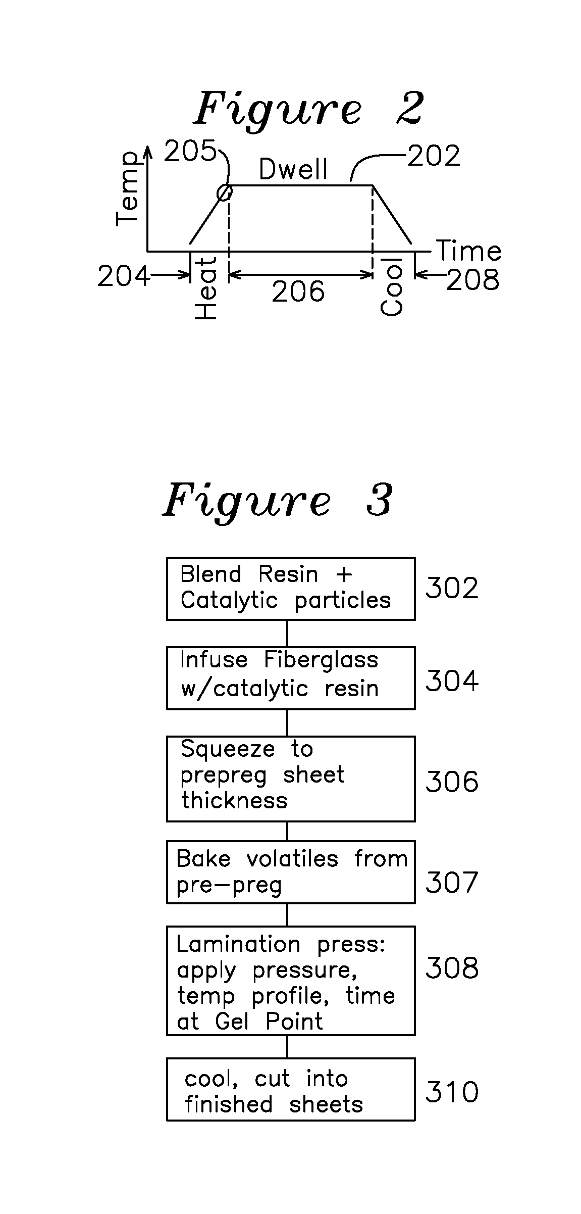
[0053]FIG. 1A shows an example process for fabricating pre-preg (a matrix of pre-impregnated fibers bound in resin). Many different materials may be used for the fibers of pre-preg, including woven glass-fiber cloth, carbon-fiber, or other fibers, and a variety of different materials may be used for the resin, including epoxy resin, polyimide resin, cyanate ester resin, PTFE (Teflon) blend resin, or other resins. One aspect of the invention is a printed circuit board laminate capable of supporting fine pitch conductive traces on the order of 1 mil (25 u), and while the description is drawn to the formation of copper traces using catalysts for electroless copper formation, it is understood that the scope of the invention may be extended to other metals suitable for electroless plating and electro-plating. For electroless deposition of copper (Cu) channels, elemental palladium (Pd) is preferred as the catalyst, although selected periodic table transition metal elements, such as group ...


PUM

PropertyMeasurementUnit
Temperatureaaaaaaaaaa
Fractionaaaaaaaaaa

Abstract

A catalytic resin is formed by mixing a resin and either homogeneous or heterogeneous catalytic particles, the resin infused into a woven glass fabric to form an A-stage pre-preg, the A-stage pre-preg cured into a B-stage pre-preg, thereafter held in a vacuum and between pressure plates at a gel point temperature for a duration of time sufficient for the catalytic particles to migrate away from the resin rich surfaces of the pre-preg, thereby forming a C-stage pre-preg after cooling. The C-stage pre-preg subsequently has trenches formed by removing the resin rich surface, the trenches extending into the depth of the catalytic particles, optionally including drilled holes to form vias, and the C-stage pre-preg with trenches and holes placed in an electroless bath, whereby traces form in the trenches and holes where the surface of the cured pre-preg has been removed.

Description

FIELD OF THE INVENTION[0001]The present invention relates to a catalytic laminate and its uses in circuit board fabrication. In particular, the laminate has properties which provide for fine pitch circuit interconnects which can be formed in trenches to form circuit board layers having planar surfaces with embedded conductors.BACKGROUND OF THE INVENTION[0002]Prior art printed circuit boards (PCB) are formed using conductive metal interconnects (known as “traces”) formed on a dielectric substrate, where each surface carrying conductors is known as a “layer”. Each dielectric core has traces formed on one surface or on both surfaces, and by stacking several such dielectric cores having traces formed in them interspersed with bare dielectric layers, and laminating them together under temperature and pressure, a multi-layer printed circuit may be formed. The dielectric substrate comprises an epoxy resin embedded in a fiber matrix such as glass fiber woven into a cloth. In one prior art f...

Claims


Application Information

Patent Timeline
IPC IPC(8): H05K1/03H05K1/02H05K3/18H05K1/09H05K3/42H05K3/46H05K1/11H05K3/38
CPCH05K1/0373H05K1/0296H05K1/09H05K3/429H05K3/4632H05K1/115H05K3/422H05K1/038H05K3/387H05K3/18H05K3/181H05K1/0353H05K2201/0209H05K2201/0242H05K2201/0227H05K1/0366H05K3/182H05K2201/0376H05K2203/0716H05K1/0313
Inventor BAHL, KENNETH S.KARAVAKIS, KONSTANTINE
Owner CATLAM LLC
Why Eureka
Try Eureka