Indium electroplating compositions containing 1,10-phenanthroline compounds and methods of electroplating indium
- Summary
- Abstract
- Description
- Claims
- Application Information
AI Technical Summary
Benefits of technology
Problems solved by technology
Method used
Image

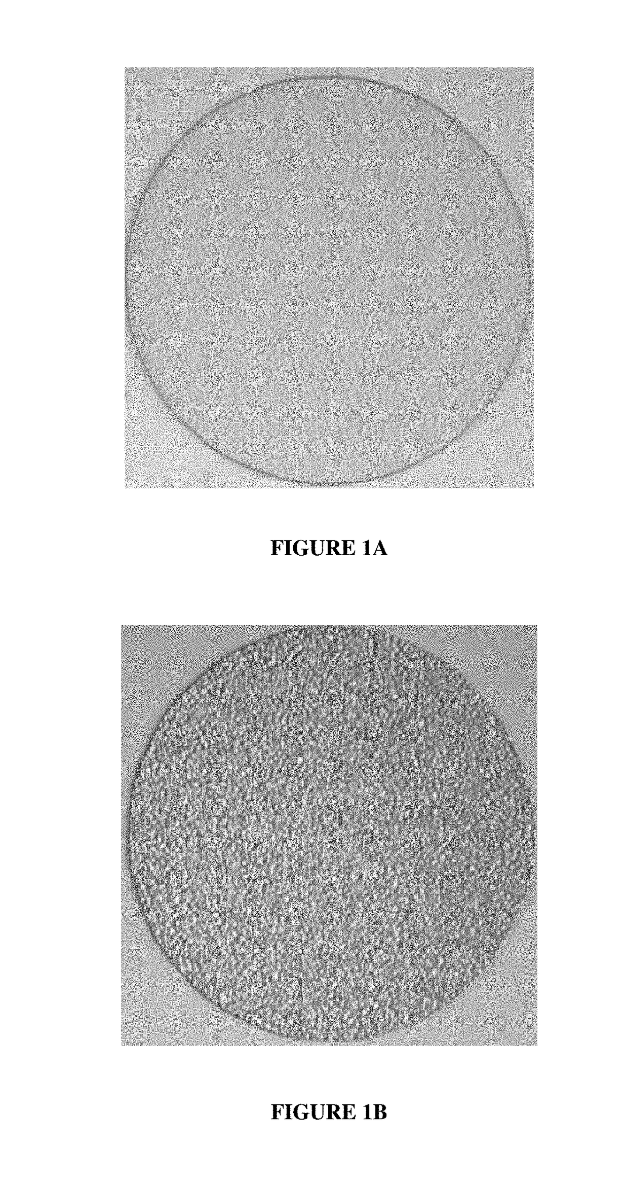
Examples
example 2
[0057]The method described in Example 1 above was repeated except that the indium electroplating composition included the following components:
[0058]
TABLE 2COMPONENTAMOUNTIndium sulfate45g / LCitric acid128g / LSodium citrate dihydrate59g / L1,10-phenanthroline8ppm
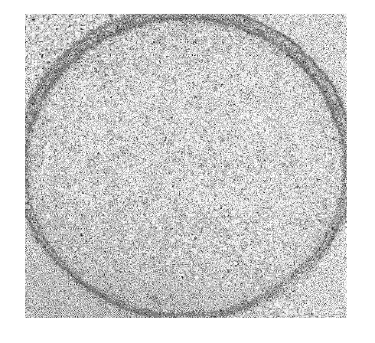
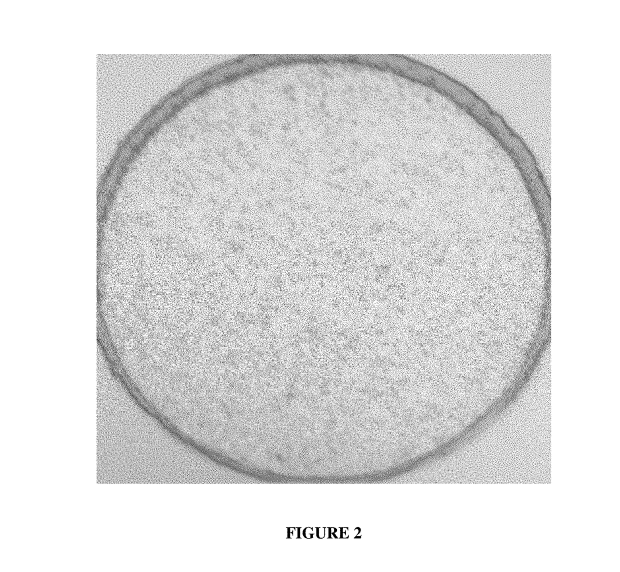
[0059]The nickel plated silicon wafers were immersed in the indium electroplating composition and indium metal was electroplated on the nickel. Indium electroplating was done at 25° C. at a current density of 4ASD for 30 seconds. The pH of the composition was 2.1. The anode was an indium soluble electrode. After indium was electroplated on the nickel layers, the photoresist was stripped from the wafers and the indium morphology was observed. All of the indium deposits appeared uniform and smooth.
[0060]FIG. 2 is an optical microscope image of one of the indium metal deposits electroplated on the nickel layer. The indium deposit appeared smooth in contrast to the indium deposit of FIG. 1B.
example 3
[0061]The method described in Example 2 above was repeated, except the indium electroplating composition included the following components:
[0062]
TABLE 3COMPONENTAMOUNTIndium sulfate45g / LCitric acid96g / LSodium citrate dihydrate59g / L1,10-phenanthroline4ppmSodium chloride150g / L1Molar ratio of chloride:indium ions = 5:1
[0063]The pH of the indium composition was 2.4. The nickel plated silicon wafers were immersed in the indium electroplating composition and indium metal was electroplated on the nickel. Indium electroplating was done at 25° C. at a current density of 4ASD for 30 seconds. The anode was an indium soluble electrode. After indium was electroplated on the nickel layers, the photoresist was stripped from the wafers and the indium morphology was observed. All of the indium deposits appeared uniform and smooth.
[0064]FIG. 3 is an optical microscope image of one of the indium metal deposits electroplated on the nickel layer. The indium deposit appeared smooth in contrast to the ind...
example 4
[0065]The method described in Example 2 above is repeated, except the indium electroplating composition includes the following components:
[0066]
TABLE 4COMPONENTAMOUNTIndium sulfate45g / LCitric acid128g / LSodium citrate dihydrate59g / L5,6-dimethyl-1,10-phenanthroline1ppm
[0067]The pH of the composition is 2.1. After indium is electroplated on the nickel layers, the photoresist is stripped from the wafers and the indium morphology is observed. All of the indium deposits are expected to appear uniform and smooth as shown in FIG. 2.
PUM
| Property | Measurement | Unit |
|---|---|---|
| Fraction | aaaaa | aaaaa |
| Fraction | aaaaa | aaaaa |
| Thickness | aaaaa | aaaaa |
Abstract
Description
Claims
Application Information
 - R&D Engineer
- R&D Manager
- IP Professional
- Industry Leading Data Capabilities
- Powerful AI technology
- Patent DNA Extraction
Browse by: Latest US Patents, China's latest patents, Technical Efficacy Thesaurus, Application Domain, Technology Topic.
© 2024 PatSnap. All rights reserved.Legal|Privacy policy|Modern Slavery Act Transparency Statement|Sitemap