Method of integration of ONO stack formation into thick gate oxide CMOS flow

a technology of oxide cmos flow and ono stack, which is applied in the field of memory cells, can solve the problems of significantly degrading the performance of a previously formed charge-trapping gate stack, adversely affecting or being impacted, and mos transistor and nvm transistor fabrication processes, so as to improve the reliability performance of nvm transistors fabricated, the effect of improving the threshold voltage (vt) uniformity and less random fluctuation of dopan

Active Publication Date: 2017-11-21
LONGITUDE FLASH MEMORY SOLUTIONS LTD
View PDF20 Cites 8 Cited by
  • Summary
  • Abstract
  • Description
  • Claims
  • Application Information

AI Technical Summary

Benefits of technology

[0059]FIGS. 3 and 4 are graphs illustrating improvements in threshold voltage (VT) uniformity of an NVM transistor according to an embodiment of the present disclosure. Referring FIGS. 3 and 4, it is shown that the reliability performance of NVM transistors fabricated according to an embodiment of the present disclosure is much improved because the ONO layers are not impacted in any way by the thick gate oxide growth of the HV MOS transistors. Th

Problems solved by technology

This integration, in some embodiments, may seriously impact both the MOS transistor and NVM transistor fabrication processes.
Charge-trapping gate stack is typically fabricated using materials and processes that differ significantly from those of the baseline CMOS process flow, and which may detrimentally impact or be impacted by the fabrication of the MOS transistors.
In particular, forming a gate oxide or dielectric of a MOS transistor may significantly degrade performance of a previously formed charge-trapping gate stack by altering a thickness or composition of the charge-trapping layer(s).
In addition, this integration may also impact the baseline CMOS process flow, and generally require a substantial number of mask sets and process steps, which add to the expense of fabricating the devices and may reduce yield of working devices.
While the HV MOS gate oxide may be formed/grown to its required thickness, since blocking or top oxide of the NVM transistor is subjected to the same environment during oxidation of the gate oxide of HV MOS transistor(

Method used


Image

  • Method of integration of ONO stack formation into thick gate oxide CMOS flow
  • Method of integration of ONO stack formation into thick gate oxide CMOS flow
  • Method of integration of ONO stack formation into thick gate oxide CMOS flow

Examples


Embodiment Construction

[0012]The following description sets forth numerous specific details such as examples of specific systems, components, methods, and so forth, in order to provide a good understanding of several embodiments of the subject matter. It will be apparent to one skilled in the art, however, that at least some embodiments may be practiced without these specific details. In other instances, well-known components or methods are not described in detail or are presented in a simple block diagram format in order to avoid unnecessarily obscuring the techniques described herein. Thus, the specific details set forth hereinafter are merely exemplary. Particular implementations may vary from these exemplary details and still be contemplated to be within the spirit and scope of the subject matter.

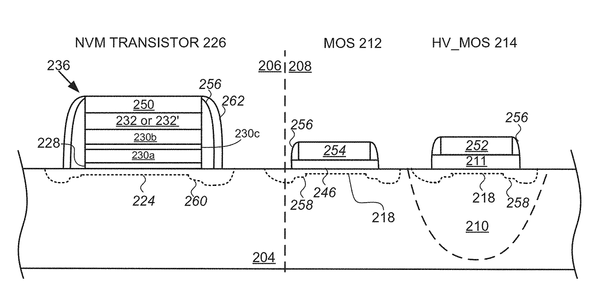
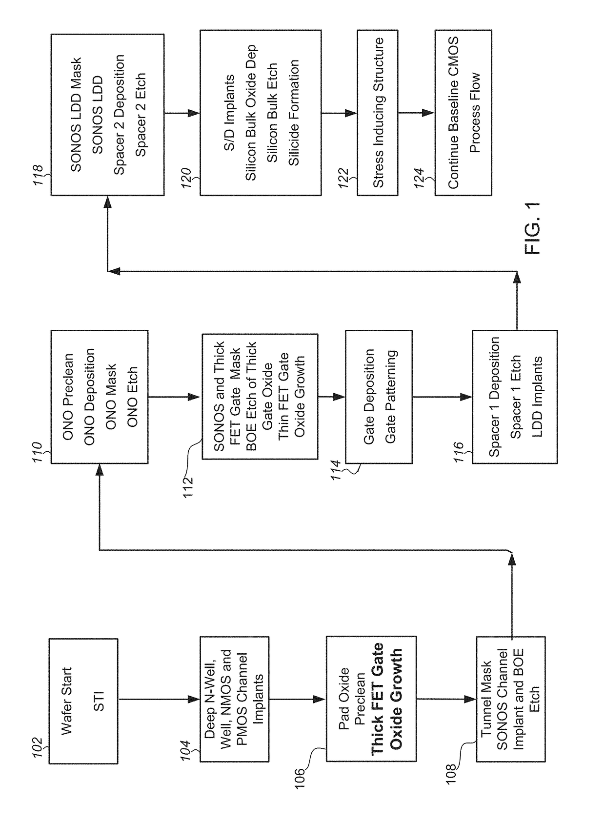
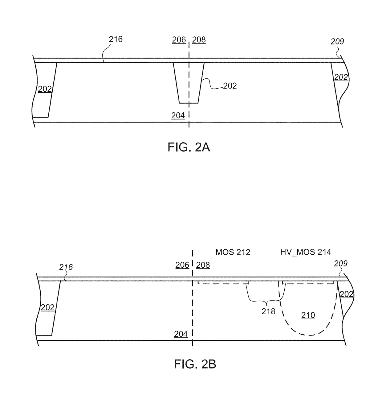
[0013]Embodiments of a memory cell including an embedded non-volatile memory (NVM) transistor and a metal-oxide-semiconductor (MOS) transistor and methods of fabricating the same are described herein with ref...


PUM


Abstract

A method of integrating a silicon-oxide-nitride-oxide-silicon (SONOS) transistor into a complementary metal-oxide-silicon (CMOS) baseline process. The method includes the steps of forming the gate oxide layer of at least one metal-oxide-silicon (MOS) transistor prior to forming a non-volatile (NV) gate stack of the SONOS transistor.

Description

PRIORITY[0001]The present application claims the priority and benefit under 35 U.S.C. §119(e) of U.S. Provisional Application No. 62 / 400,493, filed on Sep. 27, 2016, which is incorporated by reference herein in its entirety.TECHNICAL FIELD[0002]The present disclosure relates generally to semiconductor devices, and more particularly to memory cells and methods of manufacturing thereof including an embedded or integrally formed charge-trapping gate stack into an existing complementary metal-oxide-semiconductor (CMOS) foundry logic technology.BACKGROUND[0003]For many applications, such as system-on-chip, it may be desirable to integrate logic devices and interface circuits based upon metal-oxide-semiconductor field-effect transistors (MOSFET) and non-volatile memory (NVM) transistors on a single chip or wafer. This integration, in some embodiments, may seriously impact both the MOS transistor and NVM transistor fabrication processes. MOS transistors are typically fabricated using a sta...

Claims


Application Information

Patent Timeline
IPC IPC(8): H01L21/8234H01L29/66H01L21/02H01L27/11568H01L21/762H01L27/105H01L21/8238H01L29/423H01L27/092H01L27/115H01L21/28
CPCH01L21/28282H01L27/11568H01L21/76202H01L29/40117H10B43/40H10B43/35H10B43/30
Inventor RAMKUMAR, KRISHNASWAMY
Owner LONGITUDE FLASH MEMORY SOLUTIONS LTD
Why Eureka
Try Eureka