Method for preparing phase-changing film material nanometer wire
A technology of thin film materials and nanowires, applied in nanostructure manufacturing, nanotechnology, nanotechnology, etc., can solve problems such as long process cycle, high cost, and optimized process
- Summary
- Abstract
- Description
- Claims
- Application Information
AI Technical Summary
Problems solved by technology
Method used
Image

Examples
Embodiment 1
[0022] Example 1: Ge 1 Sb 2 Te 4 Nanowire preparation, the steps are
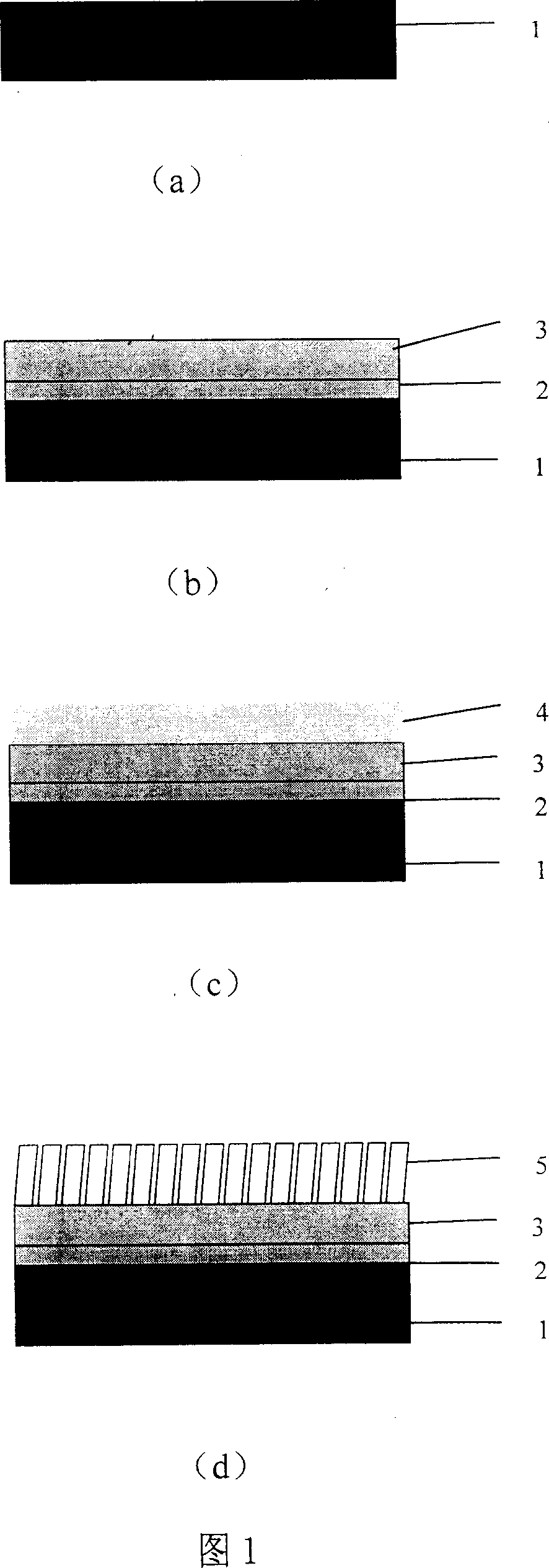
[0023] (1) Preparation of the bottom electrode: on a (100) oriented Si wafer with a diameter of 3 inches, a W / Ti electrode was prepared by using a Balzers UMS500P ultra-high vacuum electron beam evaporator. Before the evaporation starts, vacuumize to make the background vacuum reach 5×10 -7 Pa, when evaporating, due to the increase of the cavity temperature and the gas released by the evaporation source itself, the vacuum degree drops to 3×10 -6 Pa. At this time, the temperature of the substrate is room temperature, and the growth rate of the film is controlled at ~1 Ȧ. First control the electron gun to evaporate the Ti source to obtain a 20nm Ti film, and then use the electron gun to evaporate the W source to obtain a 100nm thick W film.
[0024] (2) Ge 1 Sb 2 Te 4 Preparation of thin films: Ge prepared on the bottom electrode 1 Sb 2 Te 4 alloy layer. Japan Vacuum MLH-2306 Magnetron Sputtering...
Embodiment 2
[0028] In Example 1, (1) and (2) remain unchanged in the whole film preparation process, and only changing the annealing protective atmosphere can also achieve Ge 1 Sb 2 Te 4 Nanowire formation. For annealing under argon, the pressure is maintained at 1Pa.
[0029] Ge 1 Sb 2 Te 4 The length of the nanowires can be achieved by controlling the thickness of the film. If the thickness is 1000nm, the thickness of the nanowire can be adjusted by controlling the heating and cooling speed, and also by selecting the gas and controlling the air pressure. If the heating rate is 30°C / s and the pressure is 2Pa under the protection of nitrogen, the nanowires become thinner. Adjusting the annealing temperature can also change the Ge 1 Sb 2 Te 4 The thickness of the nanowire. As in Example 1, under the condition that other process parameters remain unchanged, the annealing temperature is changed to 600° C., and the nanowire becomes thinner obviously.
Embodiment 3
[0031] (1) In Example 1, (1) and (2) are unchanged in the whole film preparation process.
[0032] (2) Prepare Ag on the bottom electrode 11 In 12 Sb 26 Te 51 alloy layer. Japan Vacuum MLH-2306 Magnetron Sputtering Apparatus is adopted, the vacuum degree is 1.1×10 -5 Pa, filled with argon to 0.8Pa. The substrate temperature is room temperature, the RF magnetron sputtering power is 150W, the sputtering time is about 5min, and the thickness is 100nm.
[0033] (3) Perform rapid annealing heat treatment in a rapid heat treatment furnace, the heating rate is 10°C / s, and after 550°C, the holding time is 1500s. The whole annealing process was carried out under the protection of nitrogen, and the pressure was kept at 1Pa.
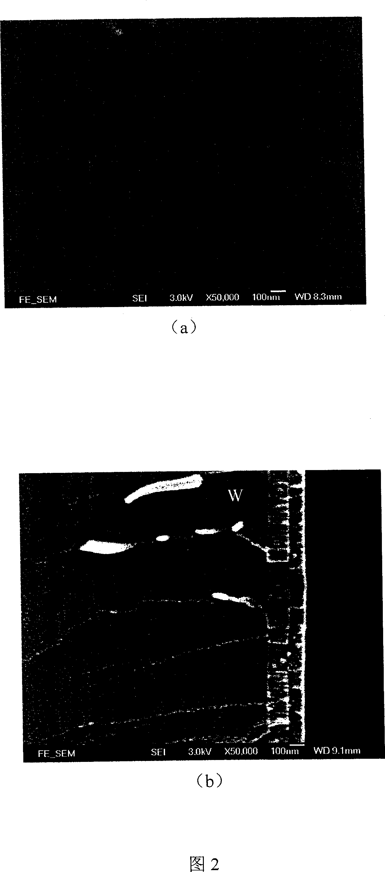
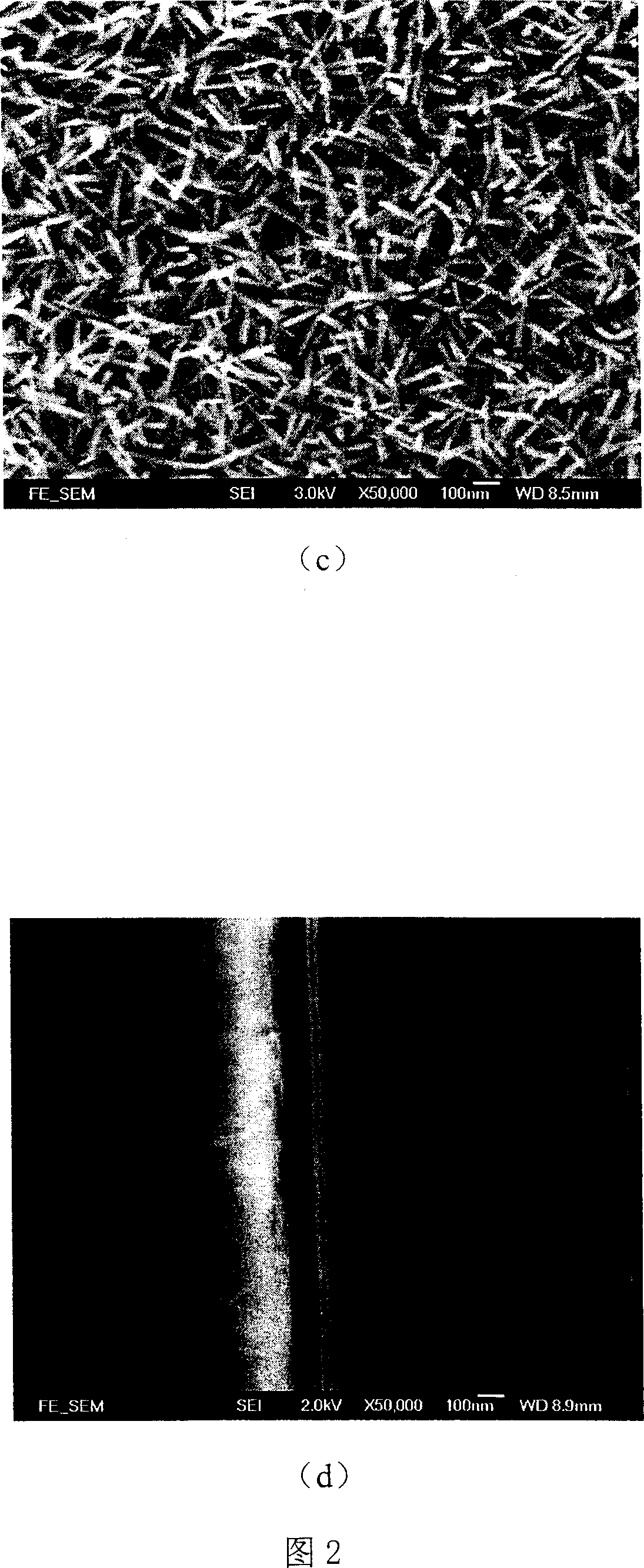
[0034] (4) SEM observation of Ag 11 In 12 Sb 26 Te 51 Nanowire formation. (similar to Figure 2)
PUM
| Property | Measurement | Unit |
|---|---|---|
| thickness | aaaaa | aaaaa |
| thickness | aaaaa | aaaaa |
| thickness | aaaaa | aaaaa |
Abstract
Description
Claims
Application Information
 - R&D
- Intellectual Property
- Life Sciences
- Materials
- Tech Scout
- Unparalleled Data Quality
- Higher Quality Content
- 60% Fewer Hallucinations
Browse by: Latest US Patents, China's latest patents, Technical Efficacy Thesaurus, Application Domain, Technology Topic, Popular Technical Reports.
© 2025 PatSnap. All rights reserved.Legal|Privacy policy|Modern Slavery Act Transparency Statement|Sitemap|About US| Contact US: help@patsnap.com