Electrochemical processing method for micro-structure of P type silicon surface

A technology of electrochemical processing and microstructure, which is applied in the field of silicon surface processing, can solve the problems of difficult general application and slow processing speed, and achieve the effects of high replication accuracy, low processing cost and fast etching speed

Inactive Publication Date: 2009-06-17
XIAMEN UNIV
View PDF4 Cites 1 Cited by
  • Summary
  • Abstract
  • Description
  • Claims
  • Application Information

AI Technical Summary

Problems solved by technology

This method is a maskless high-resolution etching method that can be used for the replication processing of three-dimensional microstructures, but its main disadvantage is that the processing rate is very slow, only 2nm / h, which determines that this technology is difficult be widely applied
[0010] In summary, so far, there is no low-cost, simple process, and suitable for the preparation of three-dimensional microstructures on silicon surfaces.

Method used


Image

  • Electrochemical processing method for micro-structure of P type silicon surface
  • Electrochemical processing method for micro-structure of P type silicon surface
  • Electrochemical processing method for micro-structure of P type silicon surface

Examples


Embodiment 1

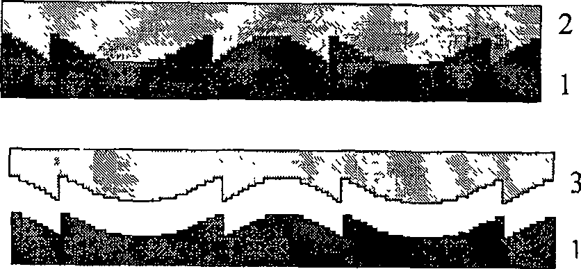
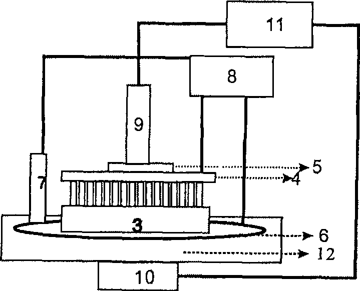
[0030] figure 1 It is a schematic diagram for preparing an agarose gel template in Example 1 of the present invention. exist figure 1 Among them, the picture above shows the thermoplastic replication process. Firstly, agarose powder and ultrapure water are mixed at a mass ratio of 1:(8-1):12, heated and dissolved, and quickly cast on the surface of the original master plate 1 with a microstructure. After removing air bubbles under vacuum and cooling for 2 hours, agarose gel 2 was formed, and the two were carefully peeled off (see figure 1 The lower figure in ) obtained agarose gel template 3 with a structure completely complementary to the original master template 1. The prepared agarose gel template 3 is generally about 2 cm long x 2 cm wide x 1 cm high. The original master 1 with microstructure can be titanium, quartz or silicon wafer with microstructure. The substrate needs to be pretreated before the experiment. Quartz and titanium only need to be ultrasonicated in acet...

Embodiment 2

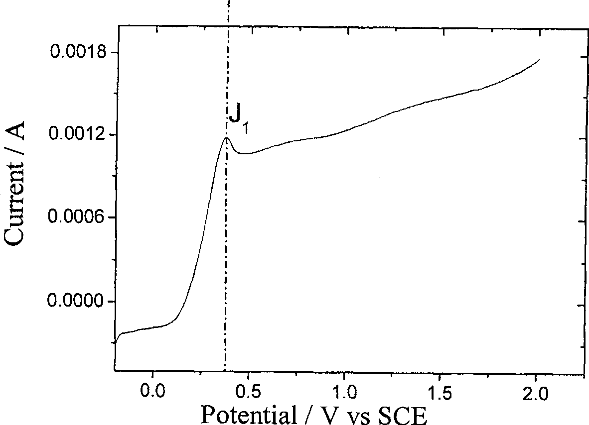
[0035] Figure 5 Micrographs and three-dimensional topography photos of the silicon surface microstructure array processed in Example 2 of the present invention are given. The electrolyte stored in the agarose gel template during processing is 0.8mol / L hydrofluoric acid, the etching potential is 1.5Vvs.SCE (saturated calomel electrode), and the processing time is 4h. The average depth of the etched pattern is 11 μm, and the etching processing speed is about 2.75 μm / h.

Embodiment 3~40

[0037] Its process steps are similar to the above-mentioned examples, and its difference lies in the concentration of hydrofluoric acid stored in the agarose gel template, and the potential of electrochemical polishing, and the specific conditions and its etching processing effect are shown in Table 1 (wherein "+" Indicates that the etching processing effect is good, "—" indicates that the etching processing effect is poor).

[0038] Table 1

[0039]

[0040] 18 0.76 1.5 + 19 0.77 1.5 + 20 0.78 1.5 + 21 0.79 1.5 + 22 0.61 1.6 + 23 0.62 1.6 + 24 0.63 1.6 + 25 0.64 1.6 + 26 0.65 1.6 + 27 0.66 1.6 + 28 0.67 1.6 + 29 0.68 1.6 + 30 0.7 1.6 + 31 0.71 1.6 + 32 0.72 1.6 + 33 0.73 1.6 + 34 0.74 1.6 + 35 0.75 1.6 + 36 0.76 1.6 + 37 0.77 0.35 — 38 0.78 0.3 — 39 0.79 0.2 — 40 0.8 0.1 —


PUM

PropertyMeasurementUnit
depthaaaaaaaaaa
depthaaaaaaaaaa

Abstract

The invention provides an electro-chemical processing method of a P-typed silicon surface micro-structure, relating to the processing of silicon surface. The invention provides a novel electro-chemical processing method which has low cost and simple processing steps, does not have complex processes such as mask lithography, etc., and with micro-structure etched and is processed on the surface of the P-typed silicon in one-step. The electro-chemical processing method comprises the steps that: the micro-structure on an original mother blank is transferred onto a gelose surface and then dipped in electrolyte, so as to gain the gelose gel template with the stored electrolyte; the gelose gel template is then arranged in an electrolytic cell, the micro-structure part of which is exposed on the liquid surface; a Pt layer is splashed on the back surface by the P-typed silicon through a front disposal to form an ohm contact; a polished surface is then arranged on the surface of the gelose gel template; the P-typed silicon sheet is taken as a working electrode and the electro-chemical polishing micro-processing is carried out to the P-typed silicon sheet; the micro-structure on the gelose gel template is transferred on the surface of the P-typed silicon by the electro-chemical polishing micro-processing to gain the P-typed silicon sheet with the micro-structure and the P-typed silicon sheet with the micro-structure is separated from the gelose.

Description

technical field [0001] The present invention relates to the processing of a silicon surface, in particular to an agarose gel template which can store electrolyte and have a microstructure combined with electrochemical polishing technology, and obtain a large-area microstructure on the p-type silicon surface by one-time replication processing A novel electrochemical machining method and its device. Background technique [0002] Silicon has become the most important basic material in microelectronics and microsystem technology because of its excellent electronic properties, mechanical and chemical properties, and it is also the most profoundly understood material so far. At present, silicon has been widely used in the microelectronics industry, and is playing an increasingly important role in the development of microsystem technology (Wang Chunhai, Yu Jie, et al. Translated. Microsystem Technology. Beijing: Chemical Industry Press, 2003). [0003] Silicon surface micromachini...

Claims


Application Information

Patent Timeline
Patent Type & Authority Patents(China)
IPC IPC(8): H01L21/3063B81C1/00
Inventor 汤儆张力庄金亮马信洲田昭武
Owner XIAMEN UNIV
Why Eureka
Try Eureka