
Method for manufacturing deep channel capacitor and etching deep channel opening

A deep trench and etching technology, applied in the manufacturing of circuits, electrical components, semiconductor/solid-state devices, etc., can solve the problems of destroying shallow trench isolation openings, residual capacitance and dielectric layers, etching uniformity and position effects, etc., to simplify the process. , the effect of large capacitance area

Active Publication Date: 2007-07-18
UNITED MICROELECTRONICS CORP
View PDF0 Cites 3 Cited by
  • Summary
  • Abstract
  • Description
  • Claims
  • Application Information

AI Technical Summary

Problems solved by technology

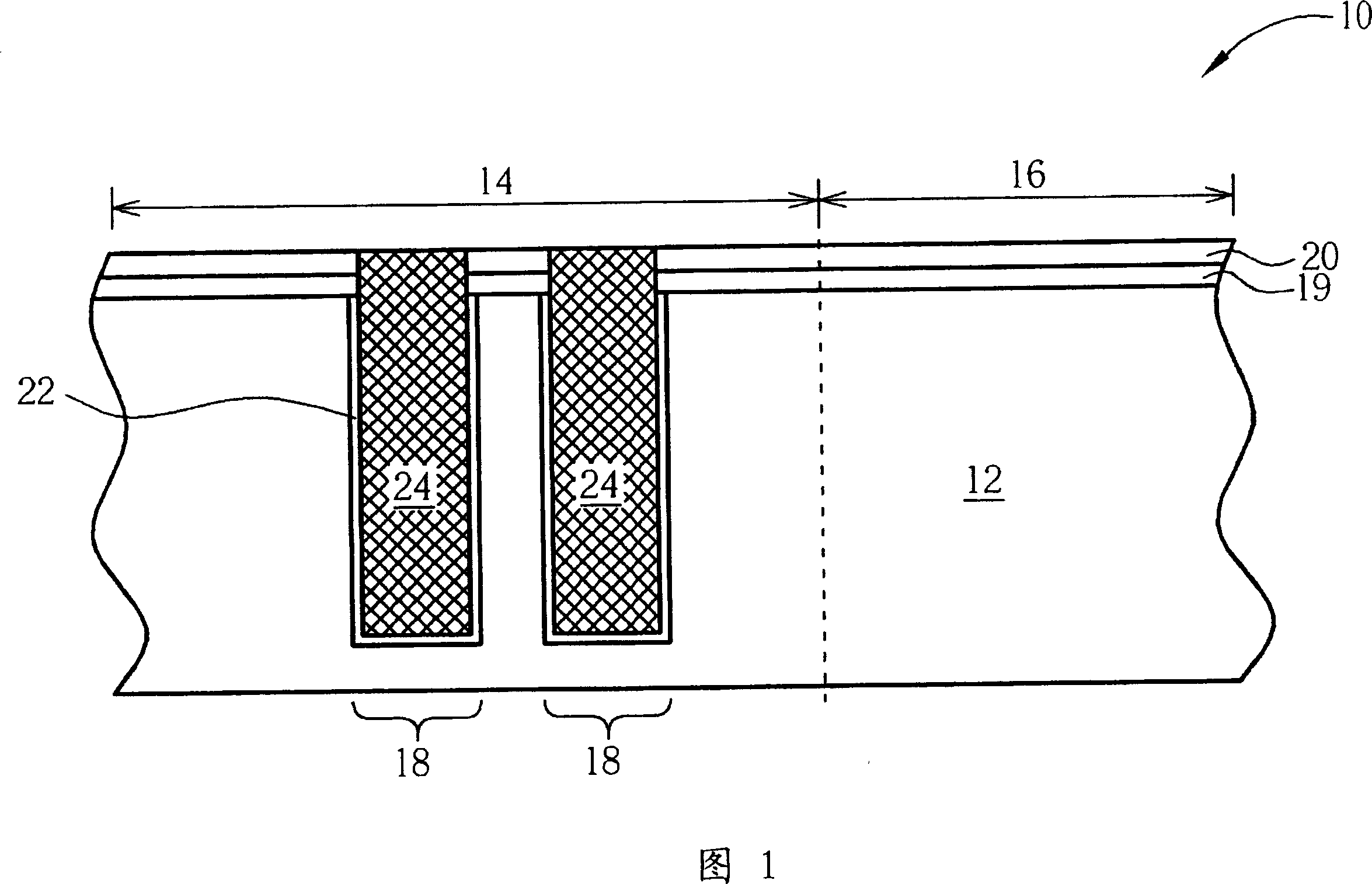
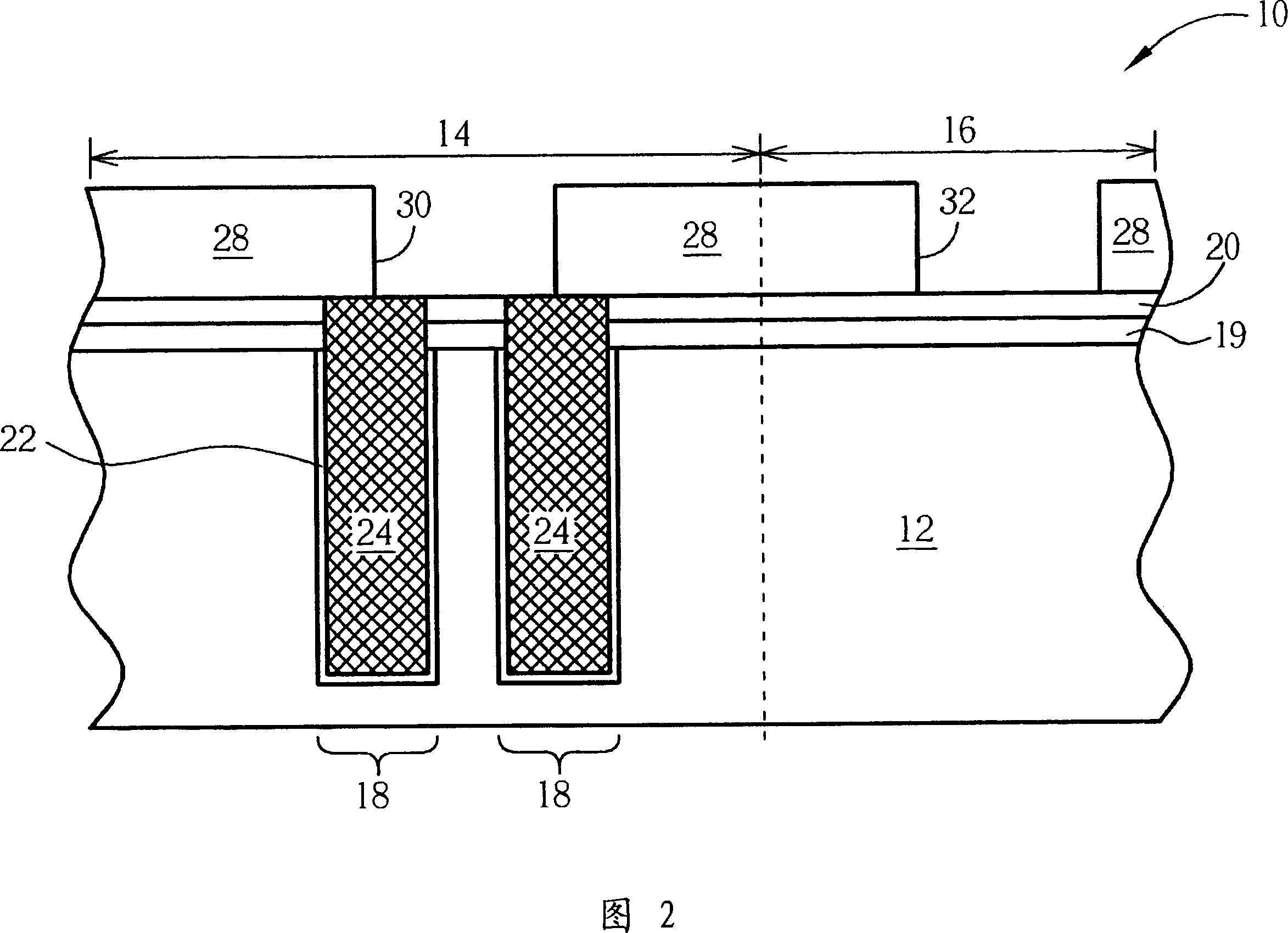
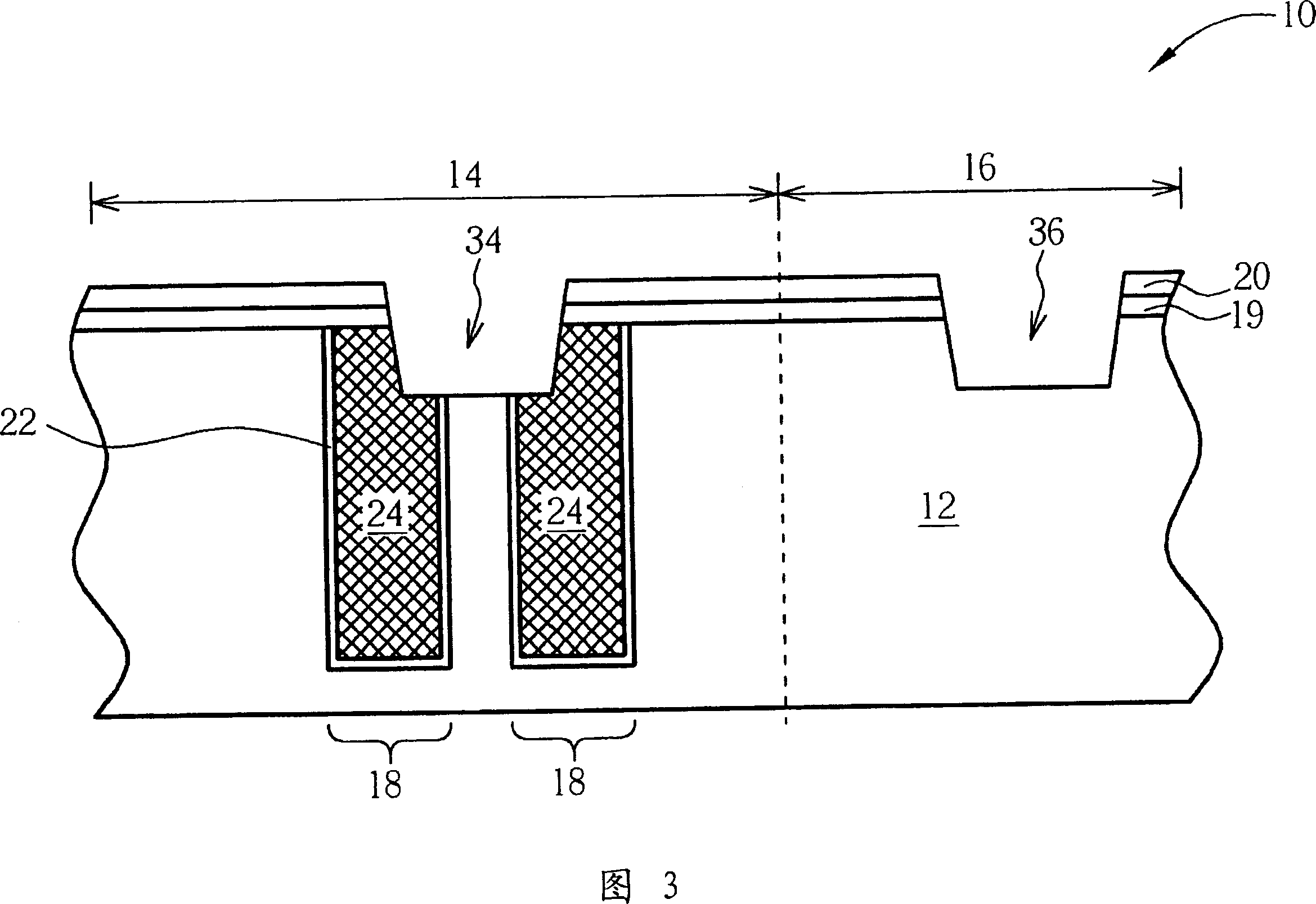
However, because the capacitor dielectric layer 22 is made of silicon oxide, silicon nitride, and silicon oxide (ONO) material, but the etching hard mask used as a deep trench opening is also made of silicon nitride, so for oxide The etching effect of the capacitive dielectric layer 22 made of silicon, silicon nitride, or silicon oxide (ONO) is not good, and it often occurs that part of the capacitive dielectric layer 22 is incompletely etched, causing the capacitive dielectric layer 52 to remain and damage the The fabrication of the shallow trench isolation opening 34
[0009] In addition, the above-mentioned method of making deep trench capacitors and shallow trench isolations using the prior art is to first fabricate deep trench capacitors and then form shallow trench isolations. However, because the shallow trench isolation openings in the logic area and memory array area on the existing semiconductor chip are It is produced together by the same etching process, and the area where shallow trench isolation openings are to be formed in the logic area only has a silicon substrate, while the area where shallow trench isolation openings are to be formed in the memory array area must etch away part of the deep trench capacitors with complex structures. Therefore, it is more difficult to control the plasma etching process of the shallow trench isolation opening, and the phenomenon of residual capacitor dielectric layer occurs, or when the logic area and the memory array area are etched with the shallow trench isolation opening at the same time, the shallow trench isolation of the logic area The etching uniformity and position of the opening are seriously affected, so it is necessary to modify the etching process through complicated computer program operations, and even multiple etching steps are required to complete the shallow trench isolation opening etching process of the logic area and the memory array area.

Method used


Image

  • Method for manufacturing deep channel capacitor and etching deep channel opening
  • Method for manufacturing deep channel capacitor and etching deep channel opening
  • Method for manufacturing deep channel capacitor and etching deep channel opening

Examples


Embodiment Construction

[0036]Please refer to FIG. 6 to FIG. 9 . FIG. 6 to FIG. 9 are schematic diagrams of forming deep trench openings according to the present invention. As shown in Figure 6, a substrate is provided, such as a silicon-on-insulator (SOI) substrate or a semiconductor chip 60, the semiconductor chip 60 is divided into a logic area 72 and a memory array area 70, and the logic area 72 and the memory array area 70 Both already have shallow trench isolation 68 . Generally, the shallow trench isolation 68 is fabricated by first depositing a silicon oxide layer 64 and a silicon nitride layer 66 on the silicon substrate 62 of the semiconductor chip 60, and then using a photomask and photolithography to etch out the shallow trenches. After the opening of the isolation 68 is filled, a dielectric substance is filled, and the fabrication of the shallow trench isolation 68 shown in FIG. 6 is completed by using a chemical mechanical polishing (CMP) process. This is well known to those skilled in...


PUM

PropertyMeasurementUnit
thicknessaaaaaaaaaa
thicknessaaaaaaaaaa

Abstract

The invention relates to a substrate, which contains an oxide silicon layer, a first nitride silicon layer, a shallow channel isolate, and the second nitride silicon layer. It forms a designed multicrystalline layer on the second nitride silicon layer, and etches the designed multicrystalline layer to form the deep ditch shedding, and then it removes the multicrystalline layer and simultaneously etches the substrate to deepen the deep channel shedding by etching method and to fill a capacitor structure into the deep channel.

Description

technical field [0001] The invention relates to a method for manufacturing deep ditch capacitors and etching deep ditch openings, in particular to a method for firstly manufacturing shallow ditch isolation layers and then etching deep ditch openings. Background technique [0002] With the trend of miniaturization of various electronic products, the current trend of making semiconductor integrated circuits is to combine dynamic random access memory (dynamic random access memory, DRAM) storage cells (memory cells) with high-speed logic circuit elements (high speed Logic circuit elements) are integrated and produced on a chip at the same time to form an embedded dynamic random access memory (Embedded dynamic random access memory) that combines a memory array and logic circuits at the same time , EDRAM), to greatly save area and speed up signal processing. [0003] In addition, the design of DRAM components must also meet the requirements of high integration and high density. T...

Claims


Application Information

Patent Timeline
Patent Type & Authority Applications(China)
IPC IPC(8): H01L21/8242H01L21/02H10B12/00
Inventor 叶大川钟倪闵黄国书林永昌李瑞池王建国
Owner UNITED MICROELECTRONICS CORP
Learn More