Micro-socle girder resonator with low temperature cross sensitivity

A technology of micro-cantilever beam and resonator, applied in the field of micro-cantilever beam resonator and cantilever beam resonator, can solve the problems of increasing the complexity and cost of chip structure, packaging and detection system, and not fully satisfying high-precision measurement, etc., to achieve The temperature compensation method is simple and easy, the structure is simple, and the effect of low cost

Inactive Publication Date: 2007-10-31
CHINA JILIANG UNIV +1
View PDF0 Cites 15 Cited by
  • Summary
  • Abstract
  • Description
  • Claims
  • Application Information

AI Technical Summary

Problems solved by technology

However, the introduction of the reference cantilever beam needs to establish an independent closed-loop circuit for it, which also greatly increases the complexity and cost of the chip structur

Method used


Image

  • Micro-socle girder resonator with low temperature cross sensitivity
  • Micro-socle girder resonator with low temperature cross sensitivity
  • Micro-socle girder resonator with low temperature cross sensitivity

Examples


Embodiment 1

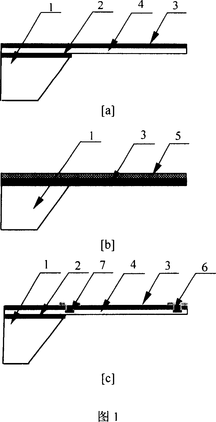
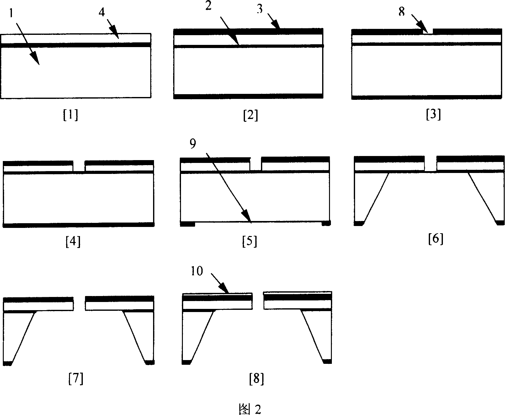
[0022] This embodiment is to manufacture a silicon / silicon dioxide cantilever beam resonator for photothermal excitation / optical signal detection. Wherein, the thickness of the silicon layer [4] is 1.3 microns, and the thickness of the silicon dioxide layer [3] is 1 micron, and its structure is shown in Figure 1(a). Its production process is as follows (see accompanying drawing 2):

[0023] (1) The original silicon wafer is a {100} double-sided polished SOI silicon wafer with a thickness of 400 microns. If the thickness of the silicon dioxide buried layer [2] is t microns, the thickness of the silicon layer [4] should be (1.8+0.45t) microns. (See Figure 2.[1])

[0024] (2) Thermal oxidation, the thickness of the oxide layer [3] is (1+t) microns. (See Figure 2.[2])

[0025] (3) The pattern of the cantilever beam is photolithographically etched on the front, and the silicon dioxide mask in the forming groove [8] around the beam is corroded by slow-release hydrofluoric acid (...

Embodiment 2

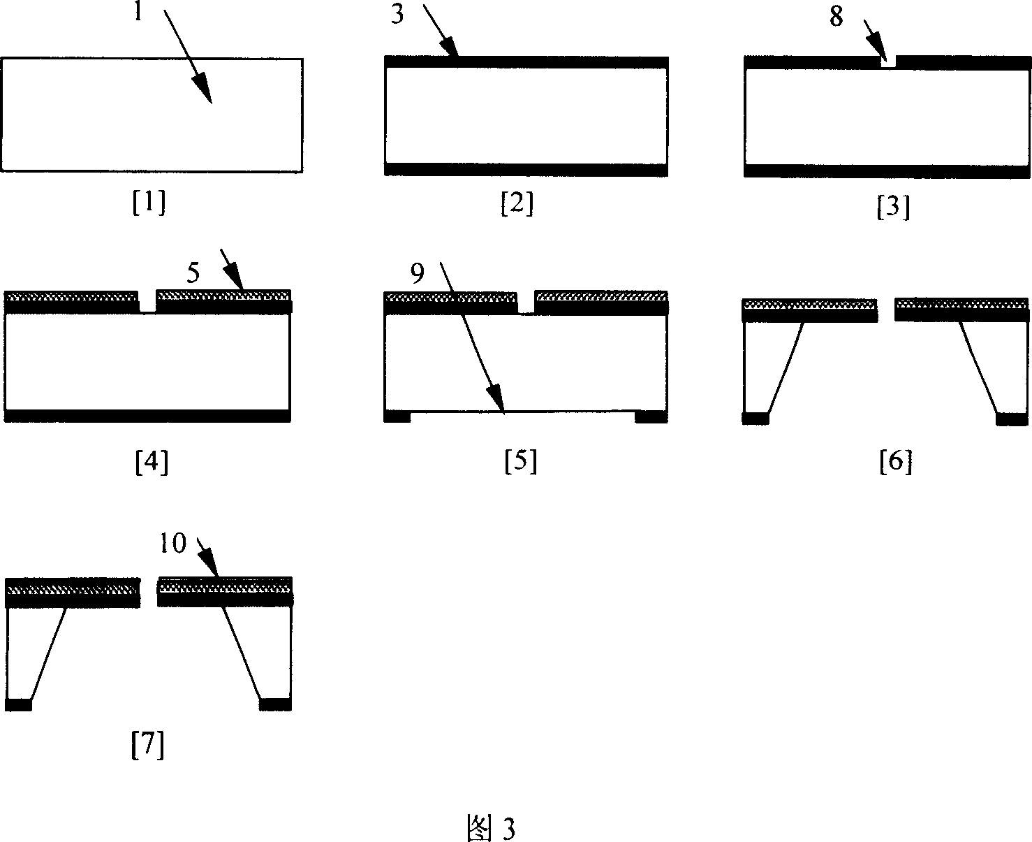
[0032] This embodiment is a silicon dioxide / silicon nitride cantilever beam resonator for photothermal excitation / optical signal detection. Its structure is shown in Figure 1(b). Its manufacturing process is as follows (see accompanying drawing 3):

[0033] (1) The original silicon wafer is an ordinary silicon wafer with {100} plane [1]. (See Figure 3.[1])

[0034] (2) thermal oxidation. (See Figure 3.[2])

[0035] (3) Photoresist protection on the back side, cantilever beam pattern photolithography on the front side, and slow-release hydrofluoric acid (BOE) corroding the silicon dioxide in the forming groove [8] around the beam. (See Figure 3.[3])

[0036] (4) LPCVD deposited silicon nitride film [5], the thickness of which is 0.9 to 1.2 times the thickness of the silicon dioxide layer [3]. For backside photoresist protection, use the same mask to etch the cantilever beam pattern on the front side, and etch away the silicon nitride film [5] in the forming groove [8] aro...


PUM

PropertyMeasurementUnit
Thicknessaaaaaaaaaa
Thicknessaaaaaaaaaa

Abstract

This invention discloses one micro hanging arm resonance device with low frequency temperature parameters, wherein it adopts dioxide silicon or silicon or silicon nitride double structure to realize temperature self-compensation; through theory computation and experiment it expresses optimum thickness proportion as 1. 1-1. 7 and the other proportion as 0. 9-1. 2; the diode silicon is grown by thermal oxidation method by low gas phase deposition method process.

Description

technical field [0001] The invention relates to a micro-cantilever beam resonator with low temperature cross-sensitivity, in particular to a cantilever beam resonator which realizes the temperature self-compensation of the resonant frequency by using the difference in the temperature coefficient of Young's modulus and density of different semiconductor materials, belonging to field of microelectromechanical systems. Background technique [0002] Sensors are the basis of test instruments and detection systems. Traditional sensors measure non-electric quantities such as pressure, temperature, and displacement by changing electrical quantities such as resistance, capacitance, or inductance, and output them as voltage and current signals. An A / D converter needs to be added between the sensor and the control circuit, which not only reduces the reliability, response speed and measurement accuracy of the system, but also increases the cost. The output of the resonant sensor is a f...

Claims


Application Information

Patent Timeline
IPC IPC(8): G12B21/00B81B7/00
Inventor 韩建强李青李昕欣王跃林韩安太孙延伟
Owner CHINA JILIANG UNIV
Why Eureka
Try Eureka