Field effect transistor, organic thin-film transistor and manufacturing method of organic transistor

A technology of field effect transistors and organic thin films, which is applied in the field of manufacturing field effect transistors, organic thin film transistors and organic transistors, can solve problems such as inapplicability, and achieve the effect of light weight manufacturing

Inactive Publication Date: 2008-01-16
HITACHI LTD
View PDF3 Cites 8 Cited by
  • Summary
  • Abstract
  • Description
  • Claims
  • Application Information

AI Technical Summary

Problems solved by technology

[0020] However, the discussion in Non-Patent Document 8 is only applicable to the electrode-inorganic semiconductor interface where the atomic bonds at the interface are mainly chemical bonds, and is generally not applicable to the electrode-organic semiconductor interface where the bond is relatively weak

Method used


Image

  • Field effect transistor, organic thin-film transistor and manufacturing method of organic transistor
  • Field effect transistor, organic thin-film transistor and manufacturing method of organic transistor
  • Field effect transistor, organic thin-film transistor and manufacturing method of organic transistor

Examples


Embodiment 1

[0067] In this example, the discussion of Non-Patent Document 8 is expanded, and a method of deriving the Schottky barrier Φ at the electrode-organic semiconductor interface is derived from the physical constants of the constituent elements of the electrode and semiconductor. Through theoretical calculations using first-principles calculations and electronic state measurements using scanning tunneling microscopy, for combinations as electrodes-organic semiconductors, hydrogen-terminated silicon surfaces-polythiophene polymers, gold-pentacene crystals, silver-pentacene After studying the electronic states of crystals, gold-various thiol monomolecular films, silver-various thiol monomolecular films, etc., the Schottky barrier can be generally estimated using (Eq. Φ. That is, when the carriers are electrons, the Schottky barrier Φ is given by (equation 7).

[0068] Φ=γ B ( M -χ S )+(1-γ B )E g / 2 (number 7)

[0069] Here, (number 8) to (number 10) are as follows.

[0070...

Embodiment 2

[0078] In this embodiment, an example of the CTFT transistor of the present invention is disclosed.

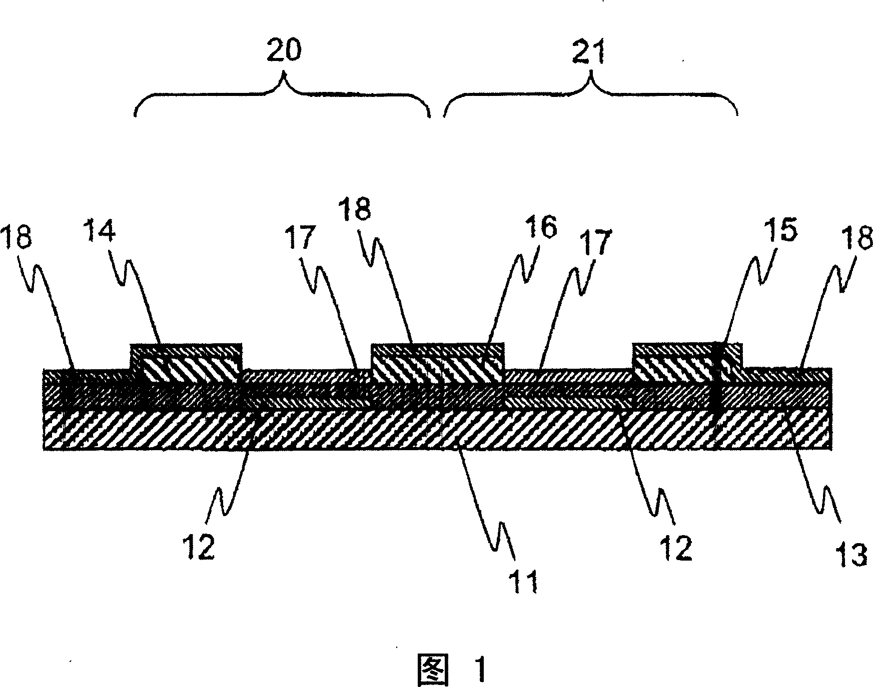
[0079] FIG. 1 is a schematic cross-sectional view showing the structure of a CTFT transistor of the present invention. In FIG. 1 , the organic semiconductor thin film 17 is a polycrystalline pentacene thin film composed of pentacene crystal grains in this embodiment. The source 14 and source 15, the organic semiconductor thin film 17, the common drain 16, and the two gates 12 constitute a CTFT transistor. The CTFT transistor is a structure in which an n-type channel FET 20 and a p-type channel FET 21 are connected in series. In this embodiment, the source 15 is a ground electrode, and the source 14 is an electrode for applying an operating voltage. On the two gates 12 A common voltage signal is input, and the drain 16 is an output electrode. The liquid repellent region 18 is a region with high liquid repellency. In the stage before the formation of the organic semiconductor ...

Embodiment 3

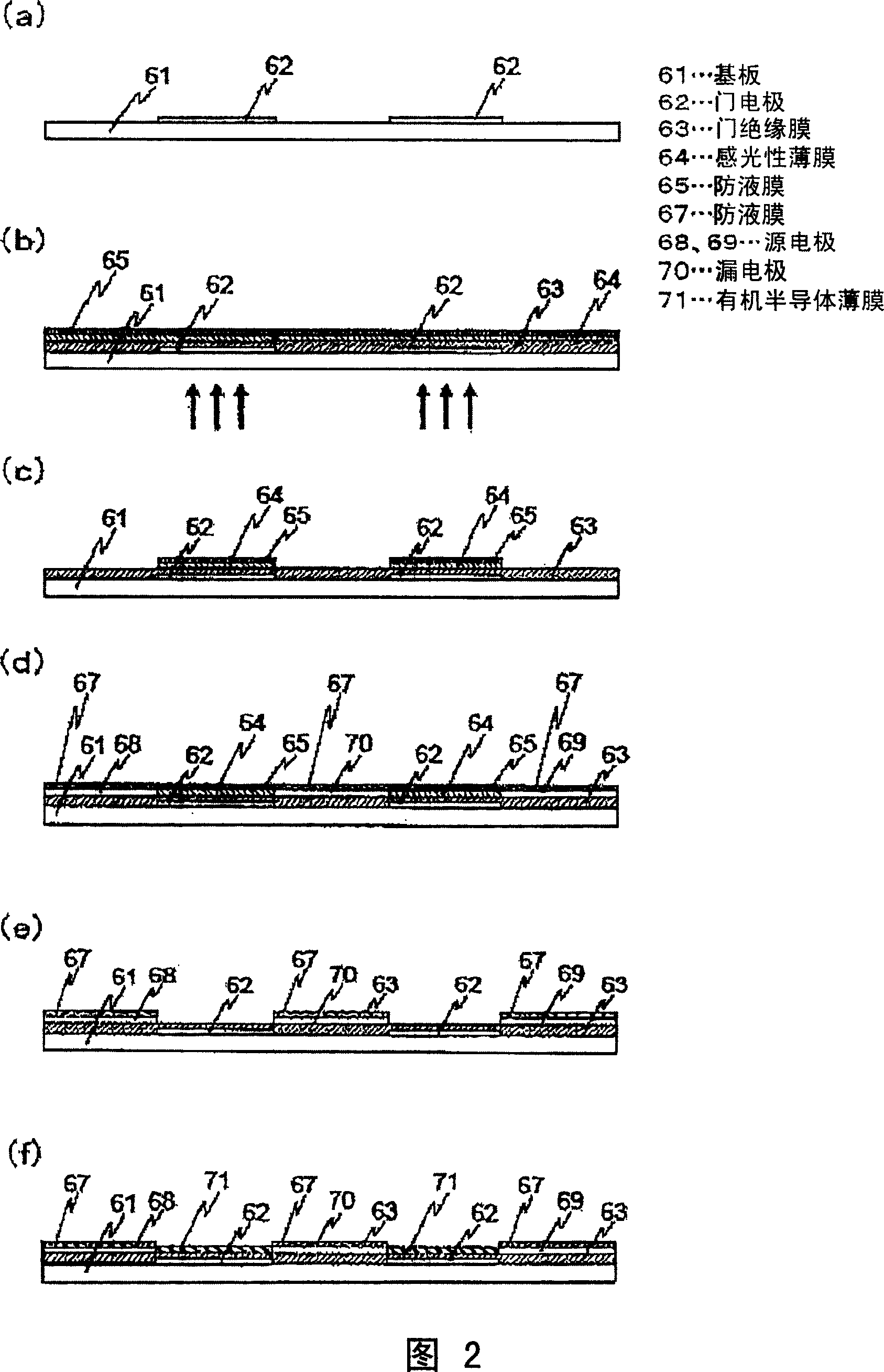
[0083] An example of a method of manufacturing a CTFT transistor formed according to the present invention is disclosed in this embodiment. FIG. 2 is a cross-sectional view showing an example of a method of manufacturing a CTFT transistor formed according to an embodiment of the present invention. In this example, a method of forming the organic thin film CTFT transistor of the present invention by printing, coating, etc., instead of lithography using a plastic material is described. 2(a)-(f) are diagrams specifically explaining the manufacturing method.

[0084] As shown in FIG. 2( a ), a gate electrode 62 is printed on a plastic substrate 61 using conductive ink. This is fired to form the gate electrode 62, but since the substrate is made of plastic, attention must be paid to its softening temperature. In this embodiment, the substrate 61 uses a highly heat-resistant and highly transparent polyimide sheet with a thickness of 100 μm, and the firing temperature can be raised...


PUM


Abstract

A method for determining the combination of the electrode and organic semiconductor with improved electron injection efficiency and hole injection efficiency in an organic TFT is provided, two types of FETs, that is, an n channel FET and a p channel FET are realized, and further, a complementary TFT (CTFT) is provided. The method for obtaining the vacuum level shift at the electrode metal / organic semiconductor interface from physical constants of constituent elements of the electrode and the organic semiconductor is provided. By changing the electrode metal through an electrochemical method, the electrodes whose electron injection and hole injection can be controlled are formed. By using these electrodes, two types of FETs such as an n channel FET and a p channel FET are realized, thereby providing a complementary TFT (CTFT).

Description

technical field [0001] The present invention relates to the manufacture method of field-effect transistor, organic thin film transistor and organic transistor, particularly relate to the thin film transistor (TFT) that has used organic semiconductor in the channel, particularly relate to the carrier that conducts in the channel into electron (n-type channel TFT) A so-called CTFT (complementary TFT) transistor in which two types of FETs (p-channel TFT) and hole (p-channel TFT) are connected in series, and its manufacturing method. Background technique [0002] In thin display devices using organic EL (Electro Luminescence) elements or liquid crystals, thin film transistors (TFTs) using amorphous silicon or polysilicon in their channels are used as elements for driving pixels. In practice, the use of amorphous silicon or polysilicon TFTs makes it difficult to have plasticity. In addition, because vacuum equipment is used in the manufacturing process, the manufacturing cost is ...

Claims


Application Information

Patent Timeline
Patent Type & Authority Applications(China)
IPC IPC(8): H01L27/28H01L21/82H01L51/05H01L51/30H01L51/40
CPCH01L51/0545H01L51/105H01L51/0021H10K71/60H10K10/466H10K10/84H10K10/481H10K10/82
Inventor 桥诘富博藤森正成诹访雄二新井唯
Owner HITACHI LTD
Why Eureka
Try Eureka