

Accurately digitized micro-nano imprint method
A micro-nano, precision technology, applied in the field of precision machining, can solve the problems of high manufacturing cost, limited function, inability to make micro-nano structures, etc., and achieve the effects of easy manufacturing, rapid imprinting and replication, and convenient replacement.
- Summary
- Abstract
- Description
- Claims
- Application Information
AI Technical Summary
Problems solved by technology
Method used
Image

Examples
Embodiment 1
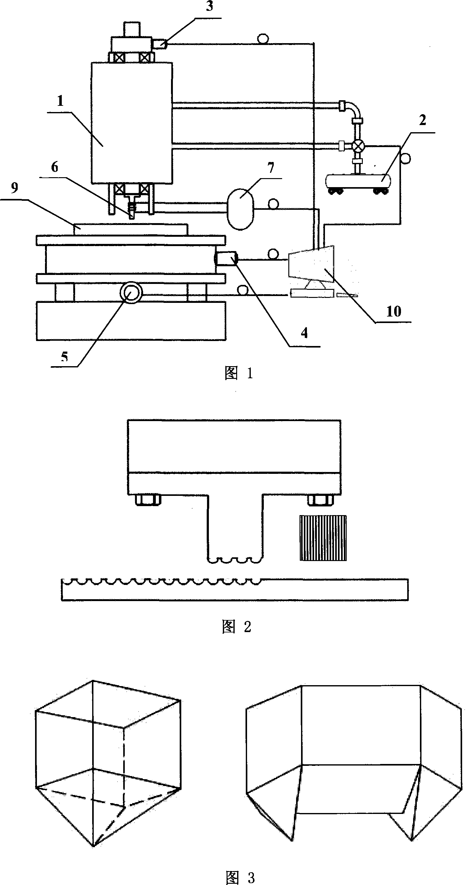
[0052] Embodiment 1: Referring to the accompanying drawing 1, a precision digital micro-nano imprinting device includes a working platform for placing a substrate 9 to be imprinted, an imprinting head 6 for installing an imprinting mold core and its driving device, and a heating and curing structure And the control device, the plane where the substrate 9 to be imprinted is located is the x-y plane, and the working platform is an x-y precision displacement working platform, which is driven by the x-axis servo motor 4 and the y-axis servo motor 5 to realize translation in the x-axis and y-axis directions Movement, the driving device of the embossing die core includes a numerically controlled rotary motion device that rotates the imprinting die core around the z-axis and a vertical translation motion device driven by the z-axis servo motor 3, and the control device provides each motion The control signal of the device, the solidification signal, and realize the pressure control. ...
Embodiment 2
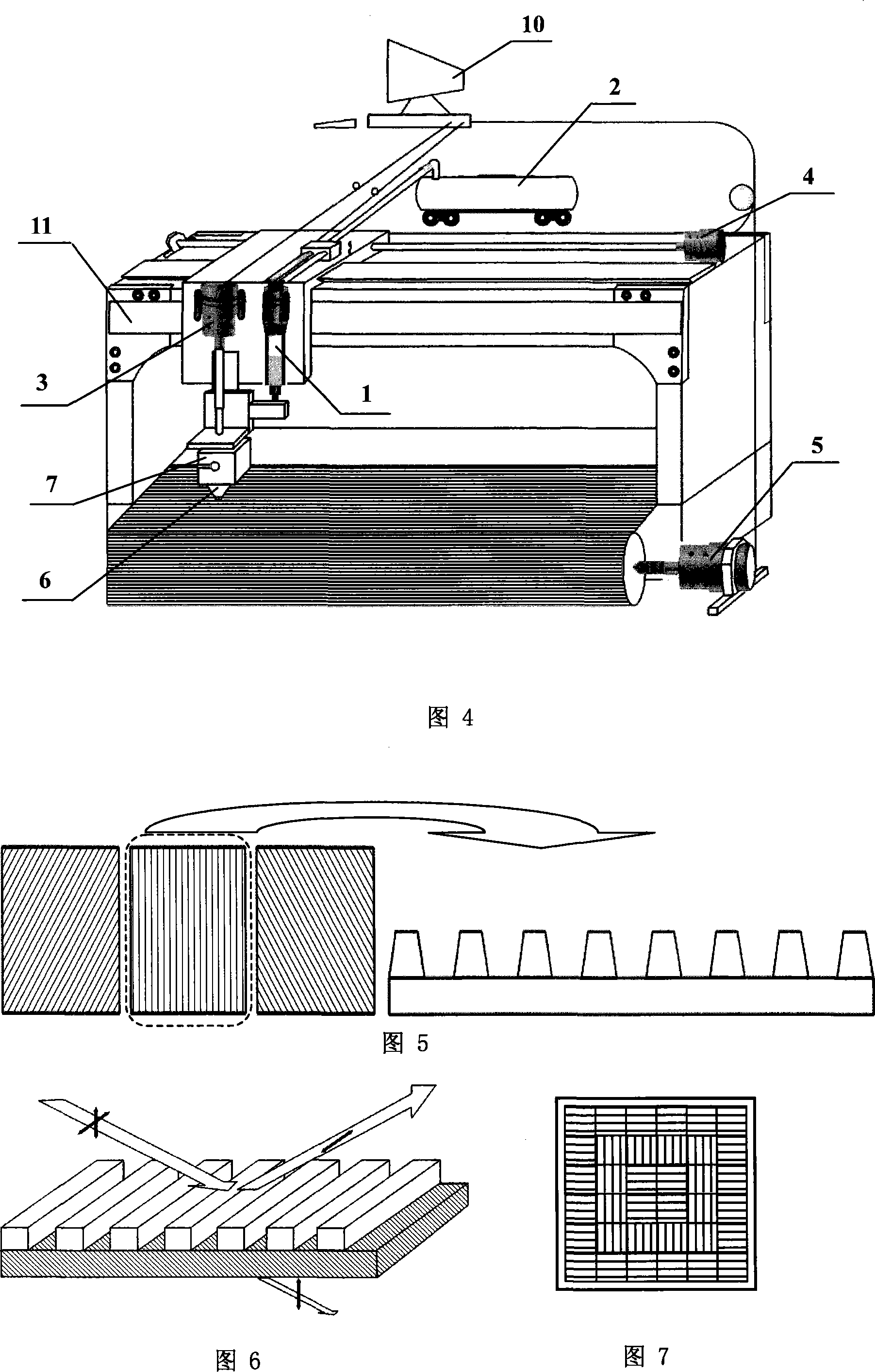
[0068] Embodiment 2: The method of precision digital micro-nano imprinting, its device is shown in accompanying drawing 4, specifically comprises the following steps:
[0069] [1] According to the actual needs, the micro-nano structure of the imprinting core unit is designed, and the finally obtained structure on the substrate is a combination of unit structures with different spatial orientations. Methods for realizing the preset micro-nano structure include ultraviolet lithography, laser direct writing, electron beam, etc. The micro-nano structure can be made directly on high-hardness materials, such as carbon steel, silicon carbide, etc., can also be made on a thin metal nickel plate, and installed on the imprint head 6 of the device.
[0070] [2] Input the spatial orientation functions of micro-nano units with different preset substrate structures into the computer 10 . The movement path of the precision displacement platform in the y direction and the embossing die core ...
Embodiment 3
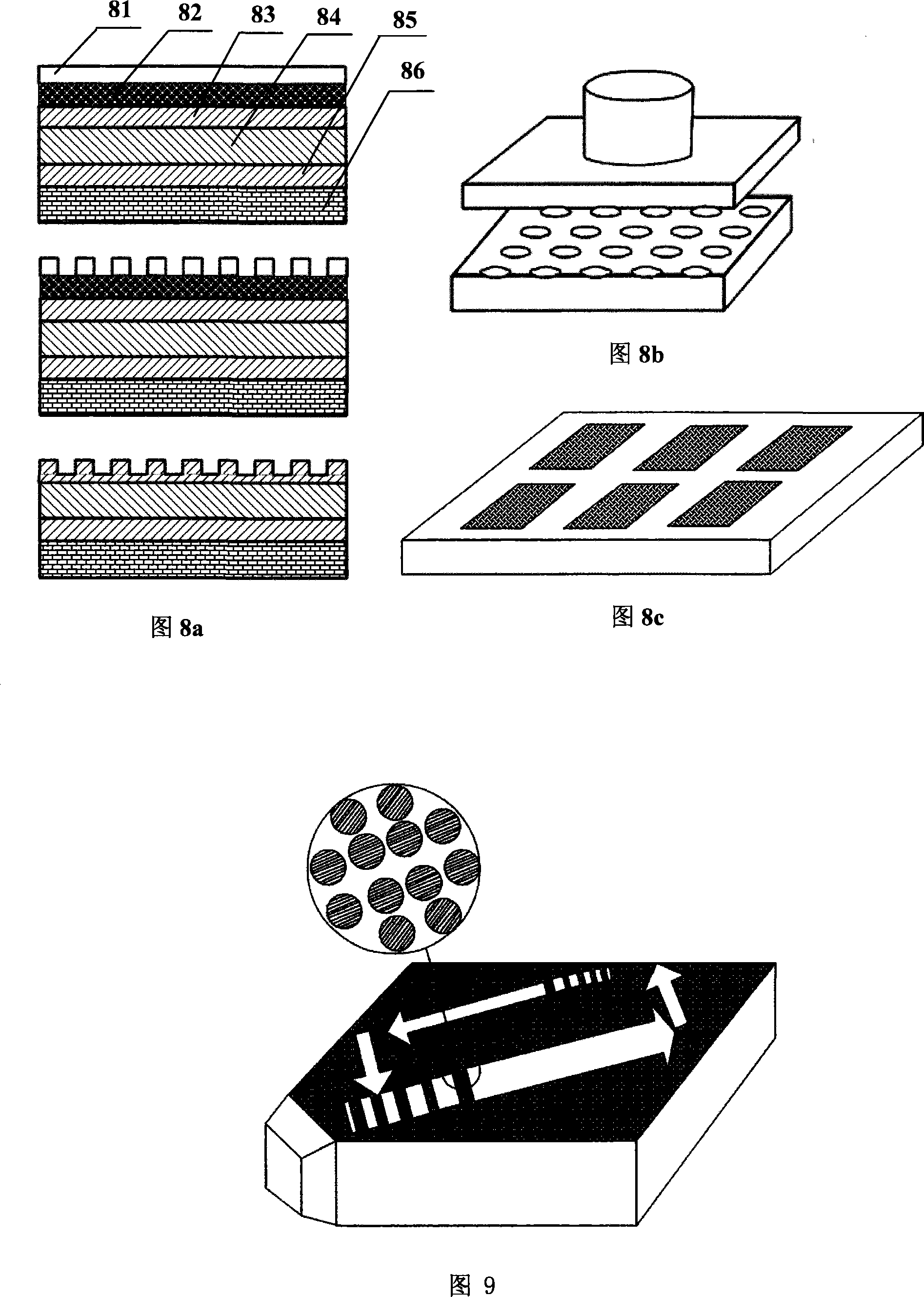
[0075] Embodiment 3: Referring to Figs. 8a-8c, a photonic crystal structure for enhancing the vertical transmission efficiency of a light emitting diode. Figure 8a is a schematic diagram of the fabrication process steps of the structure; each layer structure from top to bottom is heat-sensitive adhesive [81] / chromium mask layer Cr[82] / p-type gallium nitride layer (pGaN)[83] / quantum well Material (QW activelayer)[84] / n-type gallium nitride layer (nGaN)[85] / substrate[86], one of the implementations of the imprinting device implements embossing and primer removal on heat-sensitive materials. After etching the Cr mask [82], etch the pGaN [83] layer to obtain a periodic photonic crystal structure on the light-emitting area. Fig. 8b is a schematic diagram of the embossed structure. Figure 8c is an LED array with the photonic crystal structure.
PUM
 Abstract
Description
Claims
Application Information