Method for manufacturing variant barrier gallium nitride FET

A gallium nitride field and field effect transistor technology is applied in the manufacture of semiconductor devices, the manufacture of low gate current and high reliability gallium nitride field effect transistors, and the manufacture of variable barrier gallium nitride field effect transistors, which can solve current collapse. , increasing the distance between the gate electrode and the channel, reducing the transconductance and pinch-off voltage, etc., to achieve the effect of raising the potential barrier

Inactive Publication Date: 2008-03-19
NO 55 INST CHINA ELECTRONIC SCI & TECHNOLOGYGROUP CO LTD
View PDF0 Cites 15 Cited by
  • Summary
  • Abstract
  • Description
  • Claims
  • Application Information

AI Technical Summary

Problems solved by technology

However, these dielectric layers increase the distance between the gate electrode and the channel, reduce the transconductance and pinch-off voltage, and enhance the electric field when the channel is pinched off, and the generated high-energy hot electrons jump out of the channel, resulting in current collapse and Device performance degradation
These conflicting requirements greatly increase the difficulty of optimally designing device heterostructures

Method used


Image

  • Method for manufacturing variant barrier gallium nitride FET
  • Method for manufacturing variant barrier gallium nitride FET

Examples


Embodiment 1

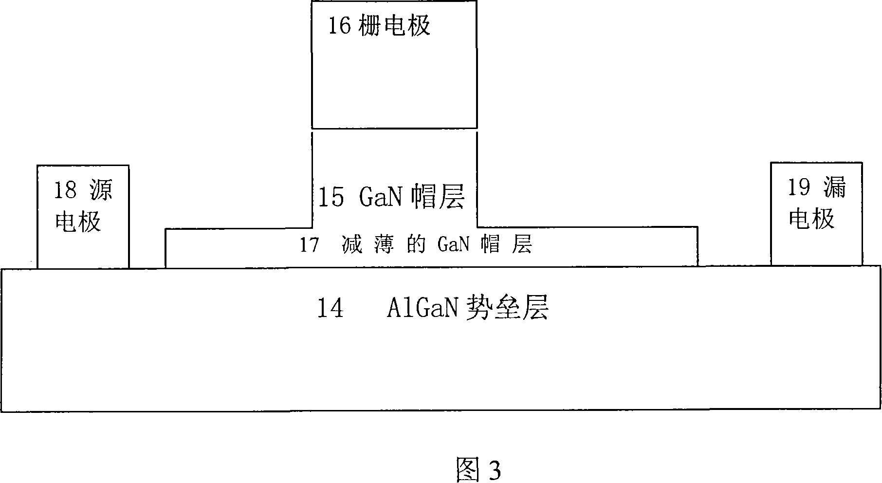
[0025] Select alloy Al with low Al composition ratio 0.04 Ga 0.96 N is the buffer layer 11, grow 10nm undoped GaN as channel layer 12, and then grow 2nm undoped AlN isolation layer 13 and 10nm undoped Al on it 0.35 Ga 0.65 The N barrier layer 14 is finally covered with an 8nm undoped GaN cap layer 15 . Self-consistently solve the Schrödinger equation and Poisson equation to calculate the channel electron gas density as 9.76*10 12 cm -2 , the pinch-off voltage is 4.2V. When the thinned GaN cap layer 17 is 3nm, the calculated electron gas density is 1.32*10 13 cm -2 . A source electrode 18 and a drain electrode 19 are fabricated on the AlGaN barrier layer 14 where the GaN cap layer has been etched completely. After removing the GaN cap layer 15, the electron gas density rises to 1.74*10 13 cm -2 . The electron gas density from the gate to the drain is 9.76*10 12 cm -2 Increased to 1.74*10 13 cm -2 Variation Barrier Field Effect Transistor.

Embodiment 2

[0026] Embodiment 2: select alloy Al with low Al composition ratio 0.04 Ga 0.96 N is the buffer layer 11, grow 10nm undoped GaN as channel layer 12, and then grow 2nm undoped AlN isolation layer 13 and 8nm undoped Al on it 0.4 Ga 0.6 The N barrier layer 14 is finally covered with an 8nm undoped GaN cap layer 15 . Self-consistently solve the Schrödinger equation and Poisson equation to calculate the channel electron gas density as 10.5*10 12 cm -2 , the pinch-off voltage is 4.1V. When the GaN cap layer is thinned to 3nm, the calculated electron gas density is 1.465*10 13 cm -2 . When the GaN cap layer is completely etched, the electron gas density rises to 2.06*10 13 cm -2 . The electron gas density from the gate to the drain is 10.5*10 12 cm -2 Increased to 2.06*10 13 cm -2 Variation Barrier Field Effect Transistor. Compared with the production example 1, after increasing the Al composition ratio of the barrier layer 14, the change span of the electron gas densi...

Embodiment 3

[0027] Embodiment 3: select alloy Al with low Al composition ratio 0.04 Ga 0.96 N is the buffer layer 11, grow 10nm undoped GaN as the channel layer 12, and then grow 2nm undoped AlN isolation layer 13 and 8nm doping concentration to 5*10 18 cm -3 Al 0.35 Ga 0.65 The N barrier layer 14 is finally covered with an 8nm undoped GaN cap layer 15 . Self-consistently solve the Schrödinger equation and Poisson equation to calculate the channel electron gas density as 1.17*10 13 cm -2 , the pinch-off voltage is 4.5V. When the GaN cap layer is thinned to 3nm, the calculated electron gas density is 1.49*10 13 cm -2 . When the GaN cap layer is completely etched, the electron gas density rises to 1.91*10 13 cm -2 . Composed from the gate to the leakage electron gas by 1.17*10 13 cm -2 Increased to 1.91*10 13 cm -2 Variation Barrier Field Effect Transistor. Modulating the doped structure increases the channel electron gas density, and making ohmic contacts on the doped laye...


PUM


Abstract

The invention provides a method for producing variant potential barrier gallium nitride field effect tube, which comprises the following steps: growing a nucleation layer, an AlGaN buffer layer and a GaN channel layer on a substrate; growing an AlN isolating layer and an AlGaN barrier layer; coating a thick GaN cap layer on the AlGaN barrier layer to increase the potential-barrier height; thinning the GaN cap layer except for the part below the grate by using chlorine-based inductively coupled plasma dry corrosion process to increase the electron gas density of the underside channel and weaken the strong field peak; performing photoetching corrosion and making a source electrode and a drain electrode on the corroded AlGaN barrier layer, to reduce the ohmic contact resistance by using the thin potential barrier and high electron gas density; and making variant potential barrier field effect tube. The invention has the advantages that the grid electrode can be formed directly on the GaN cap layer without channeling, thereby significantly reducing the gate current and improving the reliability; the fabrication of field plate electrode is omitted to simplify the process, reduce the parasitic capacitance, and increase the gain; and the invention facilitates the research of millimeter wave high-frequency apparatuses.

Description

technical field [0001] The invention relates to a method for manufacturing a semiconductor device, in particular to a method for manufacturing a variable barrier GaN field effect transistor, in particular to a method for manufacturing a GaN field effect transistor with low gate current and high reliability. It belongs to the technical field of semiconductor devices. Background technique [0002] The strong polarized charge and large energy band order on the AlGaN / GaN heterointerface generate a high-density two-dimensional electron gas, which improves the output power of GaN field effect transistors by an order of magnitude compared with GaAs field effect transistors. However, a large number of experimental studies have found that the stability of this high-power FET is very poor. In high-power radio frequency work, there is a large forward gate voltage, which generates a large forward gate current, which causes the Schottky barrier to degenerate. In addition, a strong elec...

Claims


Application Information

Patent Timeline
Patent Type & Authority Applications(China)
IPC IPC(8): H01L21/335
Inventor 薛舫时
Owner NO 55 INST CHINA ELECTRONIC SCI & TECHNOLOGYGROUP CO LTD
Why Eureka
Try Eureka