Time sharing alignment apparatus and alignment method

A technology of an alignment device and an exposure device, which is applied in the field of alignment technology and photolithography devices, can solve the problems of difficult design of an optical projection system, increased equipment cost, and high manufacturing cost, and achieves the purpose of increasing the effective imaging field of view and reducing the The effect of loading precision and reducing the difficulty of design

Active Publication Date: 2008-04-09
SHANGHAI MICRO ELECTRONICS EQUIP (GRP) CO LTD
View PDF1 Cites 9 Cited by
  • Summary
  • Abstract
  • Description
  • Claims
  • Application Information

AI Technical Summary

Problems solved by technology

[0004] In the patent CN1794095A, the exposure device in the equipment is designed for a wide band, that is, the design wavelength of the optical projection system should not only consider the wavelength of the exposure light source, but also the wavelength of the alignment light source. The chromatic aberration of the alignment band when the optical projection system is imaging, but this design idea makes the design of the optical projection system of the exposure device difficult, high in manufacturing cost and complex in assembly
At the same time, in the patent CN1794095A, since the alignment mark of the exposure object and the alignment mark of the mask are imaged onto the photodetector target surface at the same time, in order to reduce the search time of the alignment mark to improve the yield, the loading of the exposure object transmission system Accuracy puts forward high requirements, which ultimately leads to increased equipment costs

Method used


Image

  • Time sharing alignment apparatus and alignment method
  • Time sharing alignment apparatus and alignment method
  • Time sharing alignment apparatus and alignment method

Examples


Embodiment Construction

[0040]The specific embodiments of the present invention will be further described below in conjunction with the accompanying drawings.

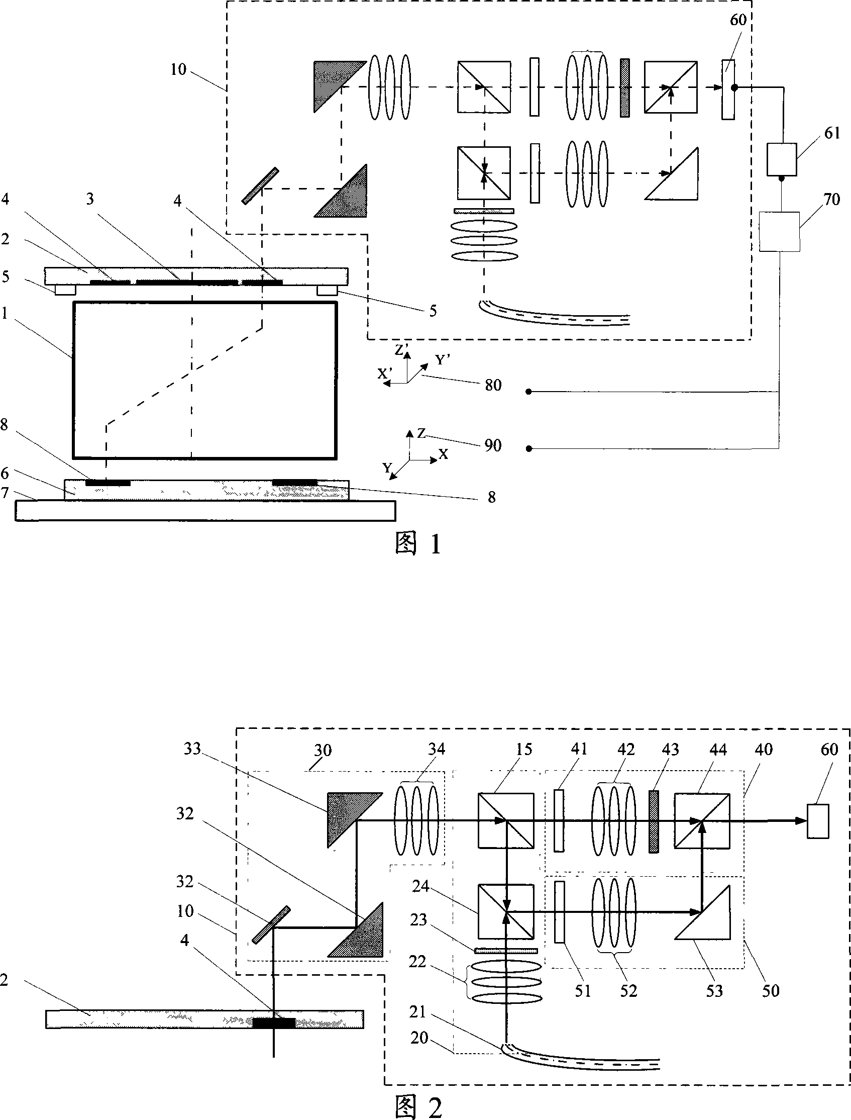
[0041] 1 shows a schematic illustration of a projection exposure device for manufacturing integrated circuits or printed circuit boards. The projection exposure device consists of an optical projection system 1, a reticle 2, a stage 5, a motion control unit 80 for the stage, and an exposure object 6. , the wafer stage 7, the wafer stage motion control unit 90, the position alignment device 10, the photoelectric detection processing unit 61 and the overall control unit 70 of the whole machine.

[0042] The reticle 2 depicting the exposure circuit pattern 3 and the mask mark 4 is placed on the plate carrier 5 and moved in X′, Y′, Z′ directions by the plate carrier motion control device 80 . The exposure object mark 8 is located on the exposure object 6, and the exposure object 6 to which the photoresist is applied is placed on the film stage 7,...


PUM

PropertyMeasurementUnit
wavelengthaaaaaaaaaa

Abstract

The present invention discloses a time-sharing alignment device and an alignment method for using the device. A mask marker imaging optical system and an exposure object marker imaging optical system are simultaneously optimized in optical structural designing, the imaging of the mask marker and the exposure marker can be carried out through different optical channels of the optical structure, and the condition of simultaneous imaging of the mask marker and the exposure marker on the surface of a photodetector is avoided by the sequential control of opening and closing of a mechanical shutter of the mask marker imaging optical system and the exposure object marker imaging optical system in view of time. The present invention reduces the designing difficulty, manufacturing cost and complex degree of the optical projection system in an exposure device.

Description

technical field [0001] The invention relates to photolithography devices in the field of integrated circuit or other micro-device manufacturing, in particular to an alignment technology and photolithography devices. Background technique [0002] In lithography packaging equipment, the pins or circuit patterns drawn on the reticle should be imaged on the surface of the exposure object coated with photoresist and other photosensitive materials through the projection exposure device. The silicon wafer where the circuit pattern will be packaged. After exposure and imaging, the silicon wafer will produce chip bumps for subsequent packaging after developing, post-baking, electroplating, ball returning and other processes. After the chip bumps are combined with the metal lead frame, they will undergo strict packaging and testing. Qualified products for user needs. [0003] Before exposing with a projection exposure device, the positions of the mask and the exposure object must be...

Claims


Application Information

Patent Timeline
Patent Type & Authority Applications(China)
IPC IPC(8): G03F7/20G03F9/00
Inventor 徐兵王鹏程吕晓薇
Owner SHANGHAI MICRO ELECTRONICS EQUIP (GRP) CO LTD
Why Eureka
Try Eureka