Mems device and fabrication method thereof

A manufacturing method and device technology, applied in the field of MEMS devices, can solve problems such as resistance value increase, mechanical strength decrease, and difficult resistance value

Inactive Publication Date: 2008-04-23
SEIKO EPSON CORP
View PDF2 Cites 7 Cited by
  • Summary
  • Abstract
  • Description
  • Claims
  • Application Information

AI Technical Summary

Problems solved by technology

[0009] As described above, in the method of implanting impurity ions into a structure made of silicon to form a diffusion layer, it is difficult to reduce the resistance value of the structure to a resistance value required for a MEMS device operating in a high frequency band
On the other hand, although the method of converting a structure made of silicon into a silicide is an effective method for greatly reducing the resistance of the structure, depending on the type of metal for silicide, it is difficult to remove a part of the wiring lamination by etching. and sacrificial layer to release the movable electrode, there is a possibility that the silicide may be partially dissolved in the etching solution
When the silicide is partially dissolved, the resistance value increases instead, or the mechanical strength decreases due to the thinning of the structure, and there is a problem that the electrical and mechanical properties of the MEMS device fluctuate and the desired properties cannot be obtained.

Method used


Image

  • Mems device and fabrication method thereof
  • Mems device and fabrication method thereof
  • Mems device and fabrication method thereof

Examples


no. 1 approach

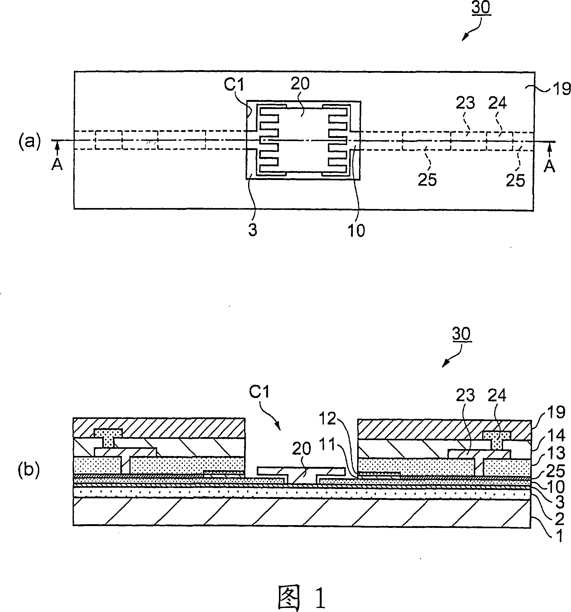
[0038] First, an embodiment of a MEMS device will be described with reference to the drawings. FIG. 1( a ) is a plan view showing the structure of a preferred embodiment of the MEMS device of the present invention, and FIG. 1( b ) is a cross-sectional view along line A-A in FIG. 1( a ).

[0039] MEMS device 30 shown in FIG. 1 has on silicon substrate 1: fixed electrode 10 provided in a fixed state; 13. The first wiring layer 23 , the second interlayer insulating film 14 , the second wiring layer 24 and the protective film 19 are formed. Furthermore, a movable electrode 20 provided in a movable state in an opening C1 serving as a space formed substantially in the center of the wiring laminated portion is provided. The surface of the portion of the fixed electrode 10 covered with the wiring lamination is converted into silicide, and a silicide portion 25 is formed.

[0040] On the silicon substrate 1, silicon oxide films (SiO 2 , for example, an insulating film 2 of a thermal...

no. 2 approach

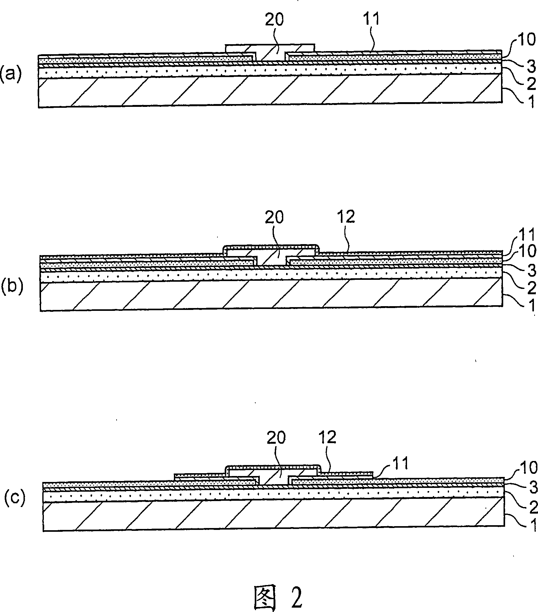
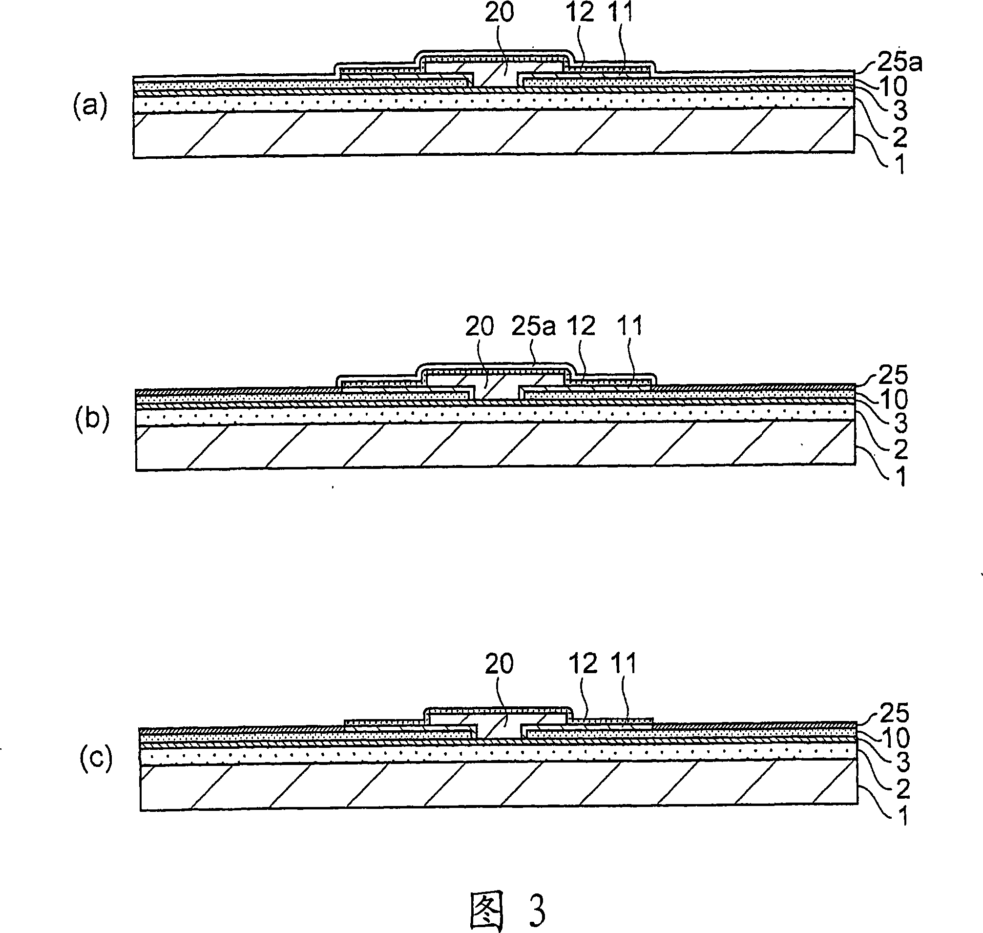
[0048] Next, a method of manufacturing the MEMS device 30 according to the first embodiment described above will be described. 2 , 3 , and 4 are schematic cross-sectional views illustrating the manufacturing process of the MEMS device 30 . 2, 3, and 4 illustrate the cross-section of the MEMS device 30 at the same position as that of FIG. 1(b).

[0049] In the fabrication of MEMS device 30, semiconductor fabrication processes are used. In FIG. 2(a), the surface of the silicon substrate 1 is thermally oxidized, etc., to form a silicon oxide film (SiO 2 ) and a nitride film 3 made of silicon nitride (SiN) or the like is deposited by CVD or sputtering. This nitride film 3 serves as a base layer functioning as an etching stopper layer when performing release etching described later.

[0050] Next, a polysilicon film is stacked on the nitride film 3 by CVD or the like, and phosphorus ions (for example, 31 P + ) and other impurity ions, the fixed electrode 10 is formed by patter...

no. 3 approach

[0066] Regarding the MEMS device 30 of the above-mentioned first embodiment manufactured by the manufacturing method of the above-mentioned second embodiment, the part of the fixed electrode 10 that is not exposed to the release of the etching solution when the movable electrode 20 is released is converted into a silicide, thereby Silicide portion 25 is formed. In contrast, in this third embodiment, an example in which a silicide portion is formed on a portion of a movable electrode and a fixed electrode exposed to a release etching solution will be described with reference to the drawings.

[0067] FIG. 5 is a schematic cross-sectional view illustrating a MEMS device 70 according to a third embodiment, and shows a cross-section at the same position as that in FIG. 1( b ) in the above-mentioned first embodiment. In addition, in the configuration of the MEMS device 70 of the third embodiment, the same configurations as those of the MEMS device 30 of the first embodiment are ass...


PUM


Abstract

The invention provides a high-performance micro electro mechanical system (MEMS) device by reducing an electrical resistance value of MEMS structures while maintaining their mechanical characteristics, and a method for fabricating the MEMS device. The MEMS device comprises: a fixed electrode (10) made of silicon and provided above a silicon substrate (1); a movable electrode (20) made of silicon and arranged in a mechanically movable manner by having a gap from nitridized film (3) of the semiconductor substrate; and a wiring layered part that is provided around the movable electrode, covers a portion of the fixed electrode. The wiring layered part comprises a first layer insulation film (13), a first wiring layer (23), a second layer insulation film (14), a second wiring layer (24) and protection film (19). A part of the portion of the fixed electrode covered by the wiring layered part is silicidized to form silicide part (25).

Description

technical field [0001] The present invention relates to a MEMS device having structures such as movable electrodes and fixed electrodes formed on a silicon substrate using a semiconductor manufacturing process, and a method for manufacturing the same. Background technique [0002] With the development of microfabrication technology, electromechanical system devices with tiny structures composed of movable electrodes and fixed electrodes formed by using semiconductor manufacturing technology, such as so-called MEMS (MEMS) such as resonators, filters, sensors, and motors Micro Electro Mechanical System (microelectromechanical system) devices have attracted much attention. Since MEMS devices are manufactured using a semiconductor manufacturing process, they can form a composite device with, for example, CMOS (Complementary Metal Oxide Semiconductor: Complementary Metal Oxide Semiconductor), so as to meet the miniaturization and high Performance-oriented devices are also expect...

Claims


Application Information

Patent Timeline
Patent Type & Authority Applications(China)
IPC IPC(8): B81B7/00B81C1/00
Inventor 稻叶正吾佐藤彰渡边徹森岳志
Owner SEIKO EPSON CORP
Why Eureka
Try Eureka