Nano contact printing
A surface contact, molecular technology, applied in nanotechnology, nanotechnology, nanotechnology for information processing, etc., can solve problems such as large amount of time, and achieve the effect of repeatability improvement
- Summary
- Abstract
- Description
- Claims
- Application Information
AI Technical Summary
Problems solved by technology
Method used
Image

Examples
Embodiment 1
[0098] Example 1: Preparation of complementary images of DNA monolayers
[0099] a. Preparation of DNA solution
[0100] Before use, wash with 75% H 2 SO 4 and 25% H 2 o 2 solution to clean all glassware. All water used was ultrapure water (18 MΩ / cm).
[0101] The first DNA 5'- / 5-thiol MC6-D / ACG CAA CTT CGG GCT CTT-3' was purchased from Integrated DNA Technologies, Inc. (IDT), Coraville, IA. All DNA strands were used as received from the manufacturer. The primary DNA was dissolved in water at a concentration of 1 μg / mL, divided into smaller aliquots of 50 μL, and stored at -20°C. When using a portion of this solution, it was reduced by placing an aliquot in 40 mM buffer solution (0.17 M sodium phosphate, pH 8) containing dithiothreitol (DTT) for 16 hr. Oligonucleotides and by-products of the DTT reaction were separated using size exclusion chromatography (NAP 10 column from Pharmacia Biotech) according to the manufacturer's instructions. 10 mM sodium phosphate buf...
Embodiment 2
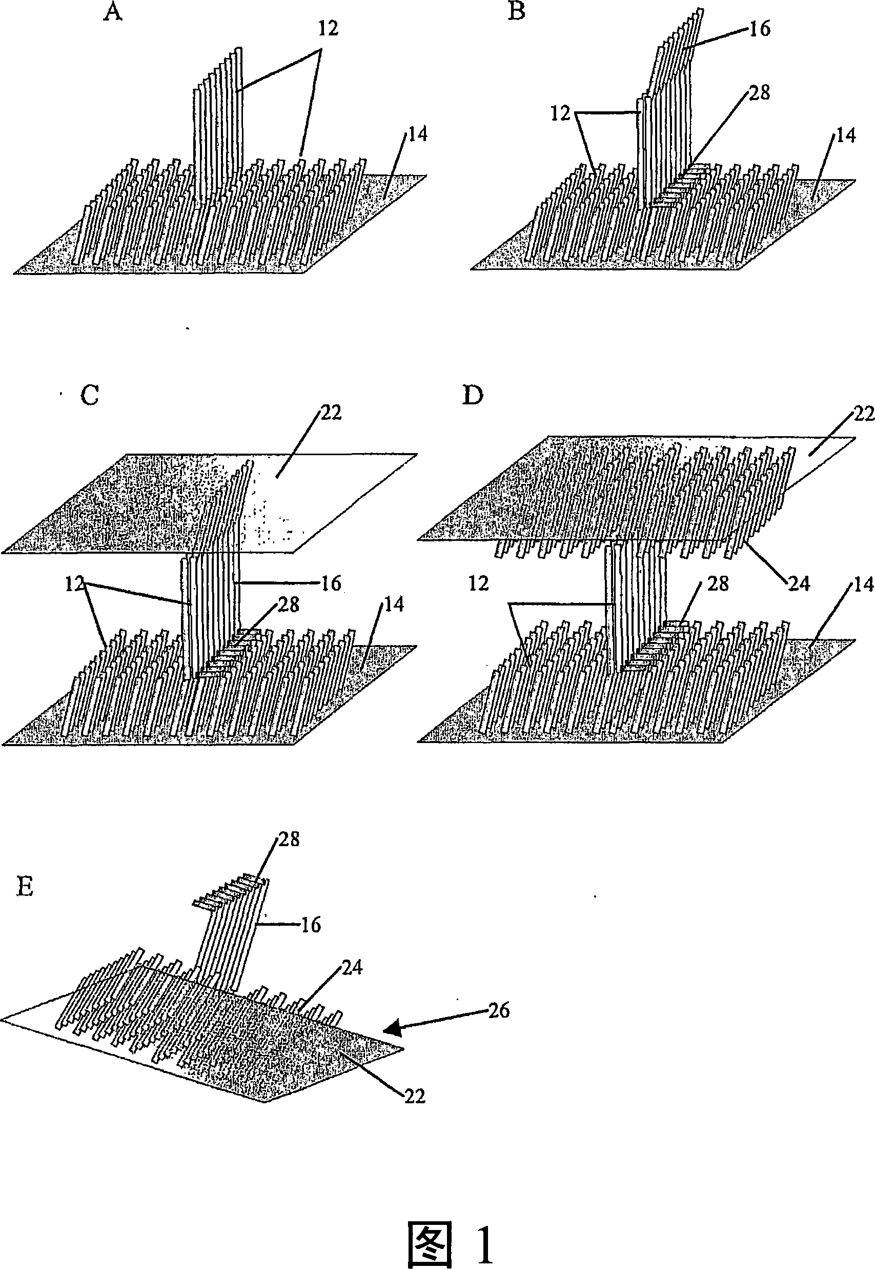
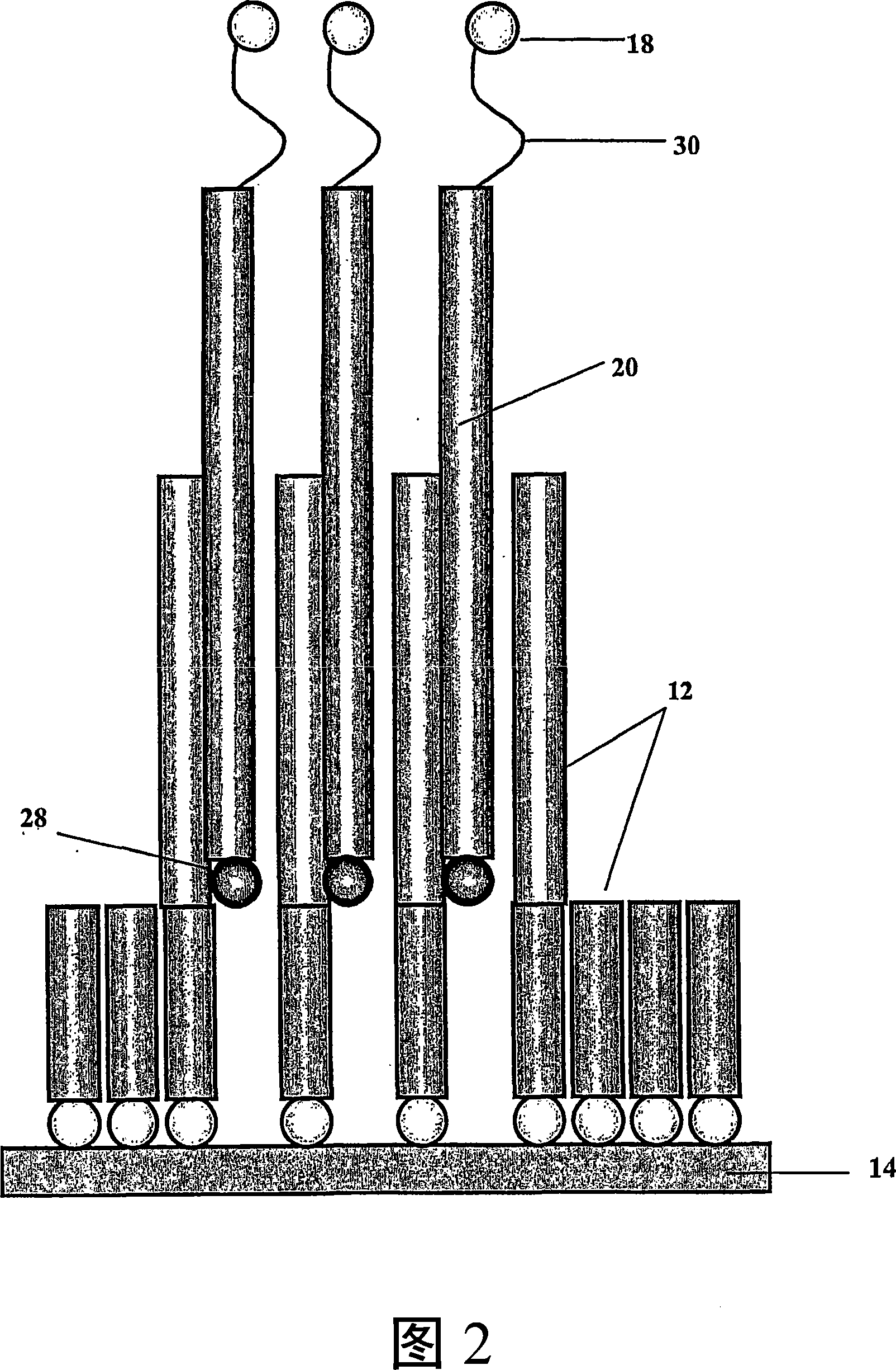
[0110] Example 2: Pattern transfer of gold grid
[0111] AFM calibrated gold grids were soaked for 5 days in a 4 μM solution of the first DNA molecule as described in Example 1 to generate a patterned body. The main body was exposed to 1 mM 6-mercapto-1-hexanol aqueous solution for 2 hr to minimize non-specific adsorption of single-stranded DNA, then rinsed 5 times with water and air-dried. Hybridization occurs by exposing the subject to a 6 μM solution of the second DNA described in Example 1 for 2 hours. The gold on second mica substrate was placed on the body so that the two gold surfaces faced each other with a small amount of water between them. A small mechanical force is applied to push the two substrates together. After about 5 hr, the substrate was soaked in 1M NaCl (70°C) in TE buffer for 20 min. The two substrates (ie, the main body and the complementary image) were automatically separated, rinsed twice with 1 M NaCl in TE buffer and five times with water, and ...
Embodiment 3
[0112] Example 3: Fabrication of DNA chips
[0113] The host was prepared using dip pen nanolithography as described by Demer et al., Angew. Chem. Int. Ed. (2001), 40:307 1-3073, the entire teaching of which is incorporated herein by reference. To prepare the host, the gold surface on the mica substrate was contacted with a 1 mM solution of 1-octadecanethiol (ODT) in ethanol for 5 min to cover the exposed gold surface with ODT molecules. The substrate was then immersed in a 1 mM solution of 1,16-mercaptohexadecanic acid (MHA) and the displacement was bound to the surface using the tip of an atomic force microscope by contacting the surface with a force of about 0.5 nN to create a 100 nm dot. ODT molecules. The MHA in solution binds to the exposed gold surfaces of the dots. Activate MHA with a 10 mg / mL solution of 1-ethyl-3-(3-dimethylaminopropyl)carbodiimide hydrochloride (EDAC) in 0.1 M morpholine / ethanesulfonic acid at pH 4.5 carboxylic acid groups, and then rinsed with...
PUM
 Abstract
Description
Claims
Application Information
 - Generate Ideas
- Intellectual Property
- Life Sciences
- Materials
- Tech Scout
- Unparalleled Data Quality
- Higher Quality Content
- 60% Fewer Hallucinations
Browse by: Latest US Patents, China's latest patents, Technical Efficacy Thesaurus, Application Domain, Technology Topic, Popular Technical Reports.
© 2025 PatSnap. All rights reserved.Legal|Privacy policy|Modern Slavery Act Transparency Statement|Sitemap|About US| Contact US: help@patsnap.com