Method for preparing gallium nitride nano-wire array by using dry etching

A nanowire array, dry etching technology, applied in nanotechnology, nanotechnology, nanostructure manufacturing and other directions, to achieve the effect of high aspect ratio, low preparation requirements, and simple electrochemical corrosion process

Inactive Publication Date: 2008-07-30
DAHOM FUJIAN ILLUMINATION TECH
View PDF0 Cites 24 Cited by
  • Summary
  • Abstract
  • Description
  • Claims
  • Application Information

AI Technical Summary

Problems solved by technology

When using porous anodized alumina as a mask to deposit Ni nanoparticle lattice, the deposited Ni nanoparticle lattice can be used as a mask to fabricate GaN nanowire arrays, but this method has not been reported.

Method used


Image

  • Method for preparing gallium nitride nano-wire array by using dry etching

Examples


Embodiment Construction

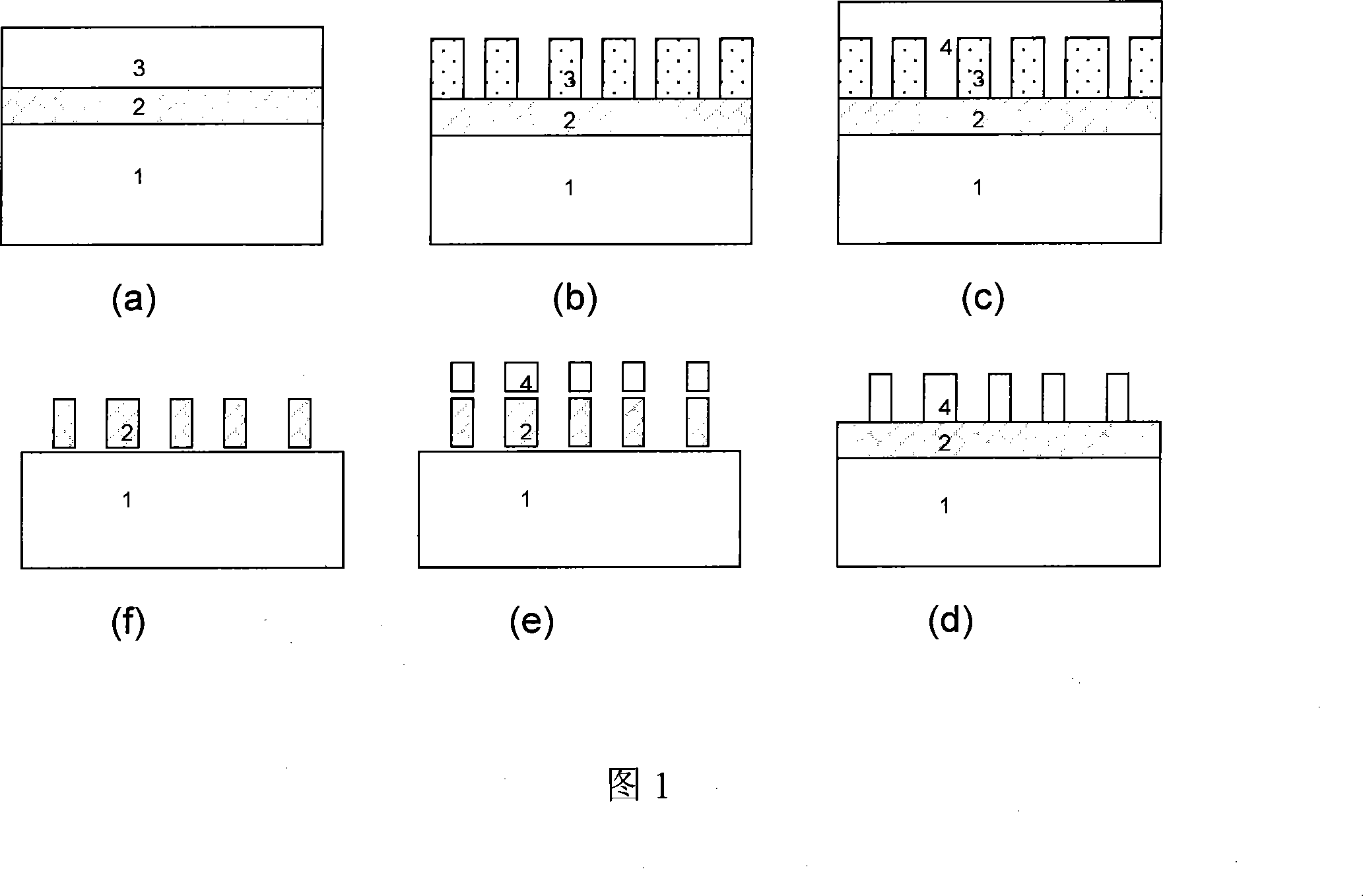
[0024] Using any one of MOCVD, HVPE or MBE methods on Al 2 o 3 4μm GaN is grown on the substrate as a template, and then a 700nm thick metal Al thin layer is deposited on the template by electron beam evaporation at a temperature of 300°C (Figure 1a), and then the template with the metal layer is placed in oxalic acid Solution (3mol / L), anodized at room temperature with a voltage of 40 volts for about 20 minutes, and then put the template into phosphoric acid solution (5wt%) and soaked for 30 minutes to remove the part of the aluminum oxide at the bottom of the hole and in contact with the lower layer of GaN , which also made a mask for depositing metallic Ni nanoparticle lattices (Fig. 1b). Next, 20 nm of Ni metal was evaporated on the template using an electron beam (Fig. 1c). Since electron beam evaporation is not selective, after removing the anodic aluminum oxide with alkaline solution (0.2mol / L NaOH solution), a lattice of metallic Ni nanoparticles will be obtained on ...


PUM

PropertyMeasurementUnit
thicknessaaaaaaaaaa
thicknessaaaaaaaaaa
thicknessaaaaaaaaaa

Abstract

The invention relates to a method for etching gallium nitride nano-wire array by using a dry method, which is characterized in that nano-particle lattice of metal Ni is taken as a mask film and the nano-particle lattice of Ni is manufactured by anodic alumina; in the manufacture of the nano-particle lattice of the GaN, first, a layer of metal As is deposited on a GaN template; second, vesicular anodic alumina is generated by adopting an electrochemical method; then, an electron beam evaporates a layer of metal Ni layer and the anodic alumina is removed by alkaline liquor. As pore arrangement and aperture size of the anodic alumina are uniform, the nano-particle lattice of the metal Ni can be obtained on the GaN template. Then, the template is placed in inductively coupled plasma or a reaction chamber reacting ion etching to be etched; at last, Ni nano-particle is removed by acid to obtain the nano-wire array of GaN. The method provided by the invention is simple and easy and the manufactured nano-wire array of GaN is applicable to the manufacture of photoelectric devices such as LED or LD.

Description

technical field [0001] The invention relates to a method for making gallium nitride (GaN) nanowire arrays by dry etching. The invention aims at making GaN nanowire arrays with high quality and high aspect ratio, and belongs to the field of GaN nanowire arrays. Background technique [0002] Low-dimensional structure semiconductor materials exhibit many excellent properties due to quantum effects, which has aroused great enthusiasm for research. Due to the confinement effect of the quantum size, the electronic energy state of the quantum wire material presents a V-shaped, T-shaped or oblique T-shaped energy level structure similar to atom splitting. Due to the separation of energy levels, quantum wire materials are more likely to meet the requirements of particle number inversion necessary for lasers, so they are suitable for making lasers. At the same time, making lasers with quantum wires will reduce the threshold current density of the laser due to the quantum confinement...

Claims


Application Information

Patent Timeline
Patent Type & Authority Applications(China)
IPC IPC(8): B82B3/00
Inventor 王新中于广辉雷本亮林朝通王笑龙齐鸣
Owner DAHOM FUJIAN ILLUMINATION TECH
Why Eureka
Try Eureka