

Application of alumina as mask for growing gallium nitride film by hydride vapour-phase epitaxial
A hydride vapor phase, epitaxial growth technology, applied in electrical components, semiconductor/solid-state device manufacturing, circuits, etc., can solve problems such as reducing the density of material growth defects, and achieve improved availability, low preparation requirements, and uniform distribution. Effect
- Summary
- Abstract
- Description
- Claims
- Application Information
AI Technical Summary
Problems solved by technology
Method used
Image

Examples
Embodiment 1
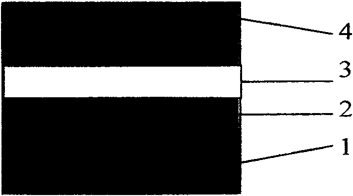
[0022] grown on Al by MOCVD 2 o 3 GaN on the substrate is used as a template, the thickness of the template is 20 microns, and then a thin layer of metal Al with a thickness of 2 μm is deposited on the template by electron beam evaporation at a temperature of 500 ° C, and then the template with the metal layer is placed in oxalic acid Solution (0.3mol / L), at room temperature using a voltage of 40 volts for anodic oxidation for 40min, and then soak the template in phosphoric acid solution (5wt%) for 30min to remove the part of the aluminum oxide at the bottom of the hole that is in contact with the lower layer of GaN, In this way, a micro-region mask for GaN growth is made. Then put the template into the HVPE reaction chamber, under N 2 The atmosphere is heated to 800°C, and NH 3 The GaN layer of the protection template is grown by HCl at 1050°C. The sample measurement results show that the dislocation density of the GaN film grown by this method is 3 to 4 orders of magnitu...
Embodiment 2
[0024] Adopt the GaN that HVPE grows on SiC substrate to make template, template thickness 100 microns, adopt the sputtering method to deposit the Al thin film of 60nm then, then make porous network aluminum oxide mask as described in embodiment 1 technique, as growth GaN mask.
Embodiment 3
[0026] Adopt MBE method to grow GaN as template on GaAs substrate, thickness is 0.5 micron, then adopt the method for growing Al thin layer as embodiment 1, Al thin film thickness is 500nm, template is placed on sulfuric acid (15wt%) solution in sulfuric acid (15wt%) earlier to carry out Anodizing, then soaking in the mixed solution of phosphoric acid and chromic acid for 30 minutes, the mixed solution is prepared from 6wt% phosphoric acid and 1.8wt% chromic acid in a volume ratio of 1:1. The dislocation density of the last grown GaN film is greatly reduced, which is similar to that described in Example 1.
PUM
| Property | Measurement | Unit |
|---|---|---|
| Thickness | aaaaa | aaaaa |
| Thickness | aaaaa | aaaaa |
| Aperture | aaaaa | aaaaa |
Abstract
Description
Claims
Application Information