Method for preparing tantalum doping tin oxide transparent conductive film
A technology of transparent conductive film and tin oxide, which is applied in the direction of ion implantation plating, metal material coating process, coating, etc., can solve the problem that the tantalum element doped tin oxide transparent conductive film has not yet been discovered, and achieve production efficiency and cost Inexpensive, strong adhesion, excellent photoelectric performance effect
- Summary
- Abstract
- Description
- Claims
- Application Information
AI Technical Summary
Problems solved by technology
Method used
Image
Examples
Embodiment 1
[0020] (1) Ta with a purity of 99.99% 2 o 5 and SnO 2 The powder is fully mixed, pressed into a billet under a pressure of 80Mpa, put into a high-temperature sintering furnace and sintered at 1650°C for 3 hours to obtain a tantalum-doped tin oxide sputtering target, in which Ta 2 o 5 The mass percentage (wt.%) is 1%, SnO 2 The mass percentage (wt.%) of the target is 99%, and the size of the target is: diameter 60mm, thickness 6mm;
[0021] (2) The prepared tantalum-doped tin oxide sputtering target is fully cleaned with analytical pure acetone and deionized water, then placed in an oven, and kept at 120°C for 3 hours to remove surface oil and other impurities;
[0022] (3) Use ordinary slide glass as the film substrate material, fully wash it with analytical pure acetone and deionized water before sputtering, then put it in an oven, and keep it warm at 80°C for 2 hours;
[0023] (4) Install and put the target material and glass slide pretreated in (2) and (3) into the mag...
Embodiment 2
[0027] Except that the composition and preparation parameters of the sputtering target are different from those in Example 1: the Ta with a purity of 99.99% 2 o 5 and SnO 2 The powder is fully mixed, pressed into a billet under a pressure of 80Mpa, put into a high-temperature sintering furnace and sintered at 1600°C for 4 hours to obtain a tantalum-doped tin oxide sputtering target, in which Ta 2 o 5 The mass percentage (wt.%) is 5%, SnO 2 The mass percentage (wt.%) of the target is 95%, and the size of the target is 60mm in diameter and 6mm in thickness;
[0028] All the other processing steps are identical with embodiment 1.
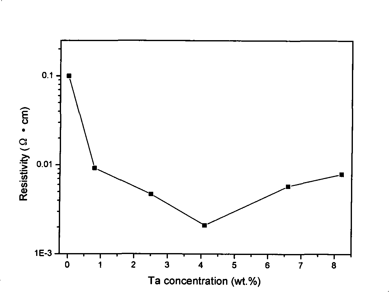
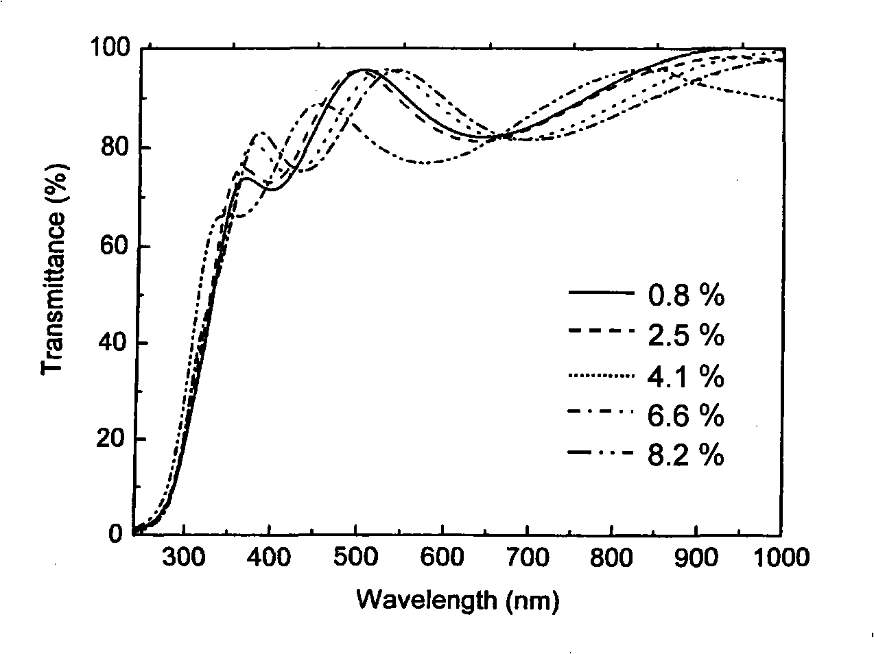
[0029] The measurement results show that the thickness of the film is about 120nm, the surface roughness (RMS) is about 4-5nm, and the resistivity of the film is 2.1×10 -3 The average transmittance of the film to visible light exceeds 90%.
Embodiment 3
[0031] Except that the composition and preparation parameters of the sputtering target are different from those in Example 1: the Ta with a purity of 99.99% 2 o 5 and SnO 2 The powder is fully mixed, pressed into a billet under a pressure of 60Mpa, put into a high-temperature sintering furnace and sintered at 1500°C for 5 hours to obtain a tantalum-doped tin oxide sputtering target, in which Ta 2 o 5 The mass percentage (wt.%) is 10%, SnO 2 The mass percentage (wt.%) of the target is 90%, and the size of the target is 60 mm in diameter and 6 mm in thickness.
[0032] All the other processing steps are identical with embodiment 1.
[0033] The measurement results show that the thickness of the film is about 130nm, the surface roughness (RMS) is about 5-6nm, and the resistivity of the film is 7.9×10 -3 The average transmittance of the film to visible light exceeds 86%.
PUM
| Property | Measurement | Unit |
|---|---|---|
| electrical resistivity | aaaaa | aaaaa |
| thickness | aaaaa | aaaaa |
| thickness | aaaaa | aaaaa |
Abstract
Description
Claims
Application Information

