Optoelectronic combination printing circuit board with optical interconnection direct coupling between chips

A printed circuit board and inter-optical technology, which is applied to the coupling of printed circuits and optical waveguides connected to non-printed electrical components, can solve the problems of difficult coupling and high alignment accuracy requirements, and achieve less optical components and easy coupling , Easy to connect and replace

Inactive Publication Date: 2009-01-14
HUAZHONG UNIV OF SCI & TECH
View PDF0 Cites 35 Cited by
  • Summary
  • Abstract
  • Description
  • Claims
  • Application Information

AI Technical Summary

Problems solved by technology

This structure uses two sets of microlens arrays to couple the optical waveguide layer and the optical transceiver device. The microlens arrays are fabricated on the chip and the printed circuit board respectively, which requires high device manufacturing and alignment accuracy and difficult coupling.

Method used


Image

  • Optoelectronic combination printing circuit board with optical interconnection direct coupling between chips
  • Optoelectronic combination printing circuit board with optical interconnection direct coupling between chips
  • Optoelectronic combination printing circuit board with optical interconnection direct coupling between chips

Examples


Embodiment Construction

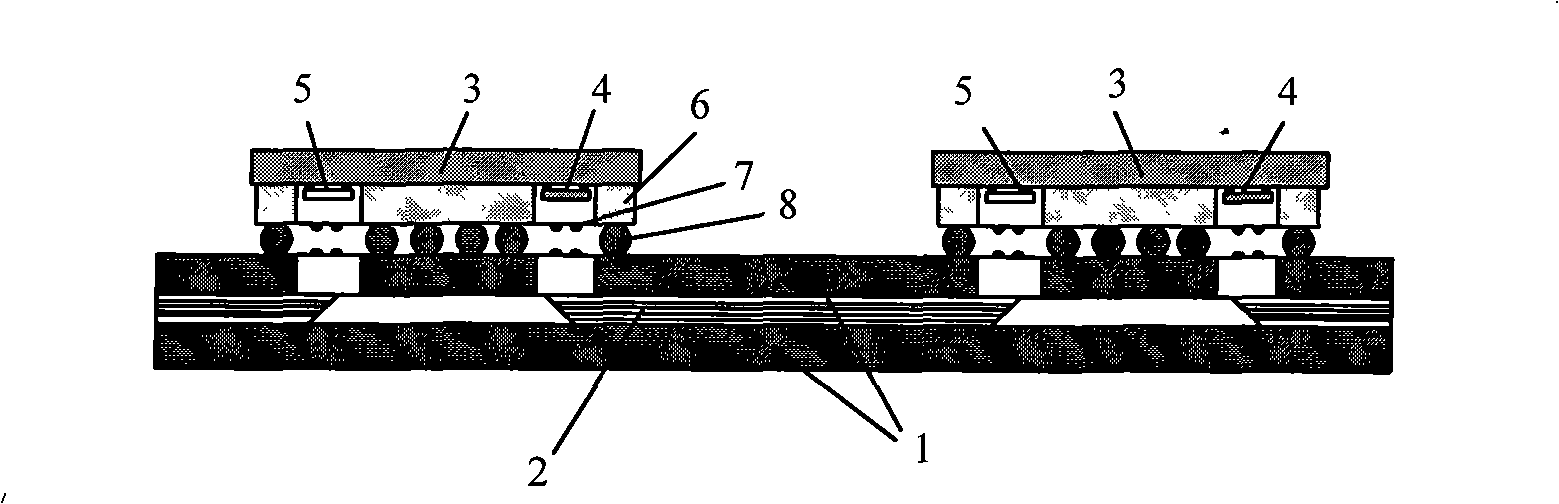
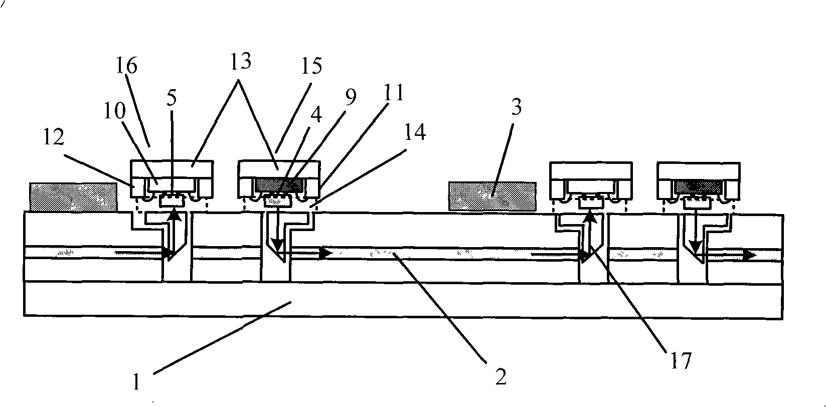
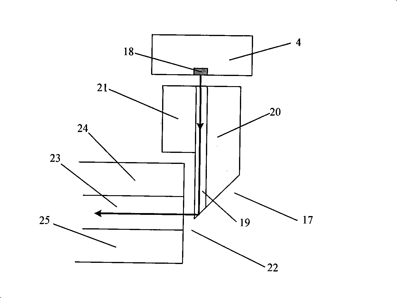
[0012] The structure of the embodiment of the present invention is as figure 2 shown. Marks in the figure: multilayer printed circuit board 1, optical waveguide layer 2, IC chip 3, VCSEL chip 4, PIN chip 5, drive circuit chip 9, transimpedance amplifier circuit chip 10, VCSEL interface circuit board 11, PIN interface circuit board 12. Copper heat sink socket 13, BGA lead pin socket 14, vertical cavity surface emitting laser device 15, PIN light receiving device 16, optical coupling connector 17.

[0013] Vertical cavity surface emitting laser device 15 is composed of VCSEL chip 4 , drive circuit chip 9 , VCSEL interface circuit board 11 bonded on copper heat sink base 13 , and BGA pin base 14 is welded on VCSEL interface circuit board 11 .

[0014] Each layer of the multilayer printed circuit board 1 is made of FR4 material, and the optical waveguide layer 2 is a polymer optical waveguide, which is embedded in the multilayer printed circuit board as an optical interconnectio...


PUM


Abstract

An optoelectronic hybrid printed circuit board provided with an inter-chip optical interconnection direct-coupling structure belongs to the photoelectron and optical communication field and aims at realizing non-lens direct optical coupling, simple-structure coupling and an optical receiving-emitting module to be pluggable for the inter-chip optical interconnection. For the invention, a laser device on the surface of a vertical cavity and a PIN optical receiver are respectively coupled in an optical manner with an optical waveguide layer of an embedded printed circuit through an optical coupling adapter formed by a lower locating plate, an optical fiber array and an upper cover plate. The optical fiber array is embedded into a parallel rectangle trough of the lower locating plate and is covered by the upper cover plate and is solidified by a UV glue; one end of the upper cover plate, one end of the lower locating plate and the optical fiber array are polished into optical planes and the other ends of the lower locating plate and the optical fiber array are all polished into 45-degree end faces. The invention just needs less optical elements and the non-lens direct optical coupling, the simple-structure coupling and the pluggable optical receiving-emitting module are all realized; the invention can be applied to the broadband, high-speed and high-capacity information communication networks and the high-capability computer process-transmission systems.

Description

technical field [0001] The invention belongs to the fields of optoelectronics and optical communication. Background technique [0002] With the continuous improvement of people's requirements for high-speed data transmission, the computer processing speed is required to develop in the direction of ultra-high-performance computer systems with petaflops and petaflops per second. Broadband, high-speed, and large-capacity information processing and transmission put forward higher requirements for interconnection speed, bandwidth, and density between printed circuit boards, between boards and backplanes, and between chips in the system. The "electrical interconnection" method of metal lines between chips on the traditional printed circuit board PCB has encountered a bottleneck. Due to its inherent serious crosstalk, RC delay, clock skew, bottleneck blocking and sharp increase in power consumption, etc., it has been unable to meet the requirements of high-speed information proces...

Claims


Application Information

Patent Timeline
Patent Type & Authority Applications(China)
IPC IPC(8): G02B6/42G02B6/24H05K1/18
Inventor 罗风光曹明翠
Owner HUAZHONG UNIV OF SCI & TECH
Why Eureka
Try Eureka