Method for preparing organic electroluminescent device

An electroluminescent device and luminescent technology, which is applied in the direction of electric solid-state devices, semiconductor/solid-state device manufacturing, electrical components, etc., to achieve the effects of increasing injection efficiency, reducing contact barriers, and wide selection range

Inactive Publication Date: 2009-02-25
UNIV OF ELECTRONIC SCI & TECH OF CHINA
View PDF0 Cites 11 Cited by
  • Summary
  • Abstract
  • Description
  • Claims
  • Application Information

AI Technical Summary

Problems solved by technology

[0005] Although OLED technology has made great progress in recent years, the curren

Method used


Image

  • Method for preparing organic electroluminescent device
  • Method for preparing organic electroluminescent device

Examples


Embodiment 1

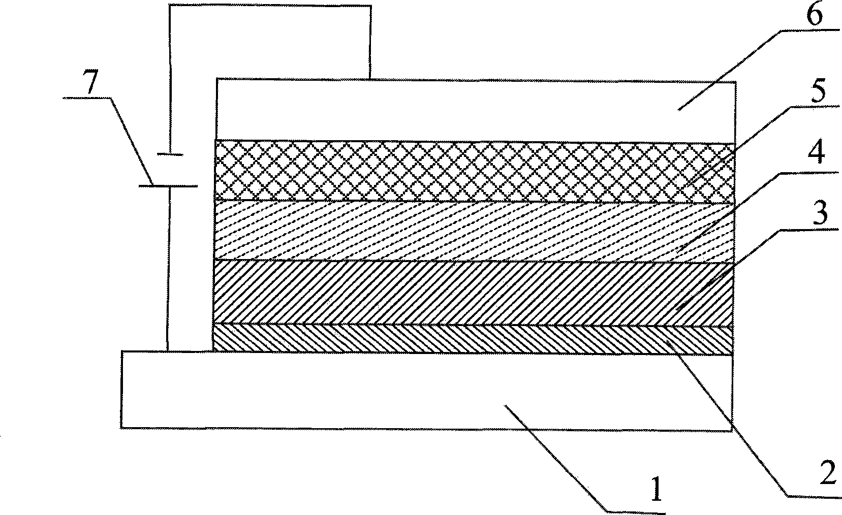
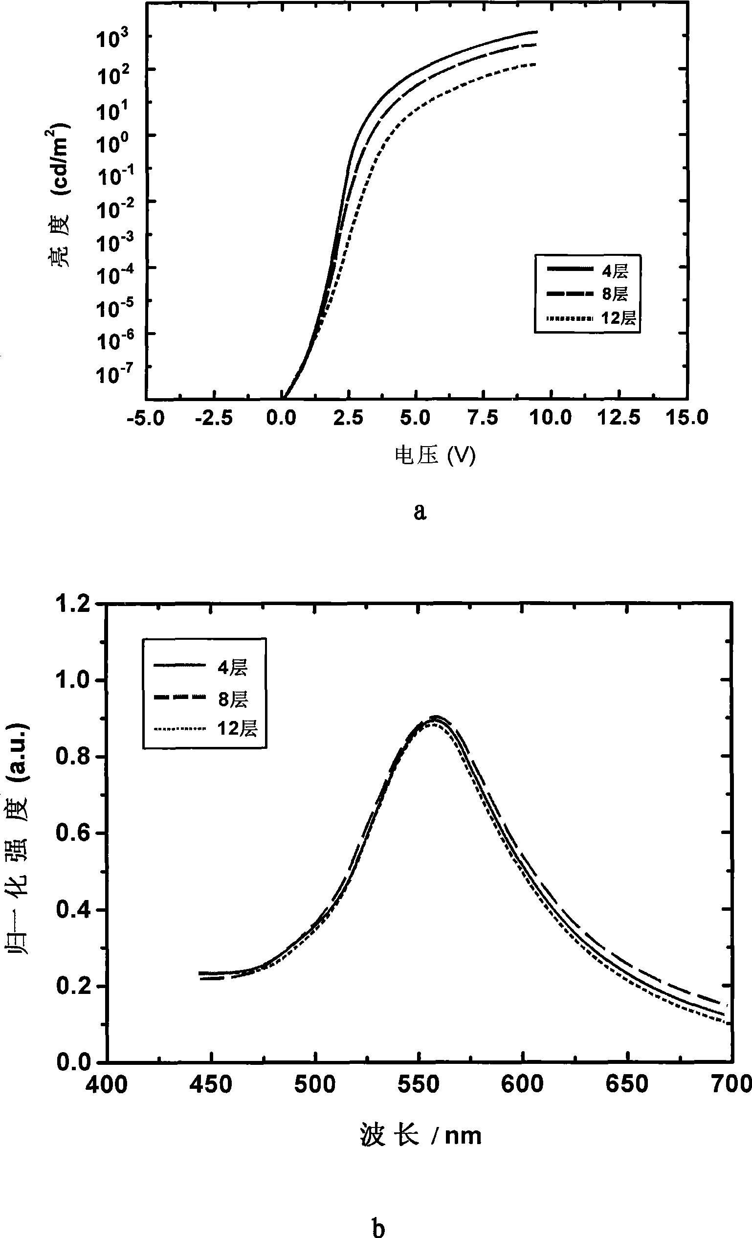
[0067] like figure 1 As shown, the organic functional layer in the device structure includes a hole transport layer 2, a light-emitting layer 3 and an electron transport layer 4, wherein the light-emitting layer 3 is a blue light-emitting layer or a green light-emitting layer, respectively.

[0068] The hole transport layer material of the device is NPB, and the light emitting layer material is BAlq or Alq 3 , the electron transport material is Alq 3 , Mg:Ag alloy for cathode layer. The entire device structure is described as:

[0069] Glass substrate / ITO / {(3,4-polyethylenedioxythiophene / polystyrenesulfonic acid) / double octadecyl chain / (3,4-polyethylenedioxythiophene / polystyrenesulfonic acid) acid)} n (n=4, 8, 12) / NPB(20nm) / BAlq(10nm) / Alq 3 (10nm) / Mg:Ag(100nm)

[0070] The preparation method is as follows:

[0071] (1) Ultrasonic cleaning was performed on the anode substrate with detergent, ethanol solution and deionized water, and after cleaning, 25% ammonia water: 30%...

Embodiment 2

[0082] like figure 1 As shown, the organic functional layer in the device structure includes a hole transport layer 2, a light-emitting layer 3 and an electron transport layer 4, wherein the light-emitting layer 3 is a blue light-emitting layer or a green light-emitting layer, respectively.

[0083] The hole transport layer material of the device is NPB, and the light emitting layer material is BAlq or Alq 3 , the electron transport material is Alq 3 , Mg:Ag alloy for cathode layer. The entire device structure is described as:

[0084] Glass substrate / ITO / {(3,4-polyethylenedioxythiophene / polystyrenesulfonic acid) / double octadecylammonium bromide chain / (3,4-polyethylenedioxythiophene / polyethylenedioxythiophene) styrene sulfonic acid)} n (n=4, 8, 12) / NPB(20nm) / BAlq(10nm) / Alq 3 (10nm) / Mg:Ag(100nm)

[0085] The preparation process of the device is the same as that of Embodiment 1

Embodiment 3

[0087] like figure 1 As shown, the organic functional layer in the device structure includes a hole transport layer 2, a light-emitting layer 3 and an electron transport layer 4, wherein the light-emitting layer 3 is a blue light-emitting layer or a green light-emitting layer, respectively.

[0088] The hole transport layer material of the device is NPB, and the light emitting layer material is BAlq or Alq 3 , the electron transport material is Alq 3 , Mg:Ag alloy for cathode layer. The entire device structure is described as:

[0089] Glass substrate / ITO / {(polyaniline / polystyrenesulfonic acid) / double octadecyl chain / (polyaniline / polystyrenesulfonic acid)} n (n=4, 8, 12) / NPB(20nm) / BAlq(10nm) / Alq 3 (10nm) / Mg:Ag(100nm)

[0090] The preparation process of the device is the same as that of Embodiment 1


PUM


Abstract

The invention discloses a method for preparing an organic electroluminescent device. The method comprises the following steps: firstly, a cationic surface active agent and a soluble ionogenic conductive polymer are assembled on the gas-liquid interface, then the laminar sequential nano structure of the conductive polymer/the surface active agent is transferred to an anode layer by the LB method to be used as the hole injection layer of the device, and then the preparation of other functional layers and an electrode film of the device is performed. Because of very good sequential laminar structure, the hole injection layer material ensures that the contact potential barrier between a hole transport layer and the anode layer is reduced, and the hole injection efficiency is enhanced. The invention can be used for the preparation of big area polymer hole injection layers to produce organic electroluminescent devices with high qualities.

Description

technical field [0001] The present invention relates to the technical field of organic electroluminescence in electronic components. Background technique [0002] In recent years, the conductive polymer poly-3,4-ethylenedioxythiophene (PEDOT) has gradually become a hot spot in the research of organic electronic materials due to its high electrical conductivity, thermal stability and good transparency. The doped PEDOT has high electrical conductivity and is a hole-rich material, so it can be used as a hole-transporting material for organic electronic devices. Afterwards, through the copolymerization method, Bayer obtained a 3,4-polyethylenedioxythiophene / polystyrenesulfonic acid (PEDOT:PSS) conductive polymer colloid with tunable conductivity and water-solubility. It has good environmental stability, good electron blocking properties and transparency, and has good affinity for ITO, making it an ideal material for hole injection buffer layers of organic electroluminescent dev...

Claims


Application Information

Patent Timeline
IPC IPC(8): H01L51/56
Inventor 蒋亚东杨亚杰于军胜徐建华
Owner UNIV OF ELECTRONIC SCI & TECH OF CHINA
Why Eureka
Try Eureka