LCD substrate, LCD and manufacturing method

A technology of a liquid crystal display and a manufacturing method, which is applied in the field of thin film transistor liquid crystal displays, can solve the problems of fracture, too large interlayer end difference, and the transparent pixel electrode cannot be normally turned on.

Active Publication Date: 2009-03-18
BOE TECH GRP CO LTD +1
View PDF0 Cites 22 Cited by
  • Summary
  • Abstract
  • Description
  • Claims
  • Application Information

AI Technical Summary

Problems solved by technology

Although the source-drain electrode contact hole 22 can be formed into a forward taper in the process, so that the transparent pixel electrode 21 can reduce the occurrence of disconnection, the thickness of the transparent pixel electrode 21 is generally only , and the slope angle 28 at the ...

Method used


Image

  • LCD substrate, LCD and manufacturing method
  • LCD substrate, LCD and manufacturing method
  • LCD substrate, LCD and manufacturing method

Examples


Embodiment Construction

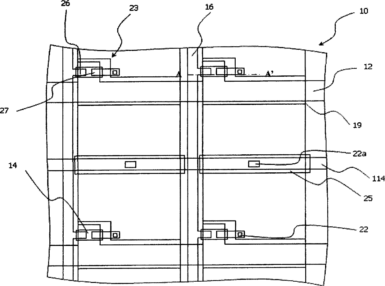
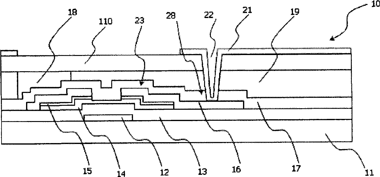
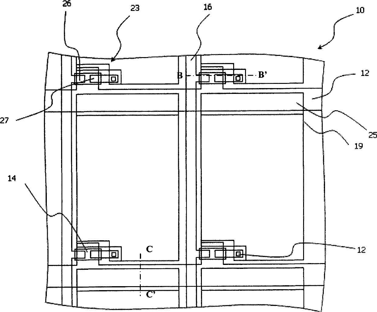
[0050] image 3 Is a top view of the pixel area of ​​the liquid crystal display substrate of the present invention; Figure 4 Yes image 3 Sectional view of B-B’; Figure 5 Yes image 3 Sectional view of C-C’. Such as image 3 , Figure 4 with Figure 5 As shown, the TFT substrate 10 of the present invention specifically includes: forming an aluminum alloy containing one or more of neodymium, silicon, copper, antimony, tungsten, tantalum, and scandium on a glass substrate 11, and forming an aluminum alloy on the glass substrate 11. A plurality of gate lines or gate electrodes 12 formed by laminating high melting point metals such as titanium, chromium, and molybdenum. An insulating gate insulating layer 13 made of oxide, nitride or oxynitride compound (such as SiNx) is formed thereon, and a data line 16 made of high melting point metal is formed by crossing the gate insulating layer 13 with the gate line. The area divided by the gate line 12 and the data line 16 forms a pixel are...


PUM


Abstract

The invention discloses a liquid crystal display device baseboard, comprising a baseboard, a gate line, a gate electrode, a gate insulation layer, an active layer, a resistance contact layer, a source cathode, a drain electrode and a data line, wherein the data line and the gate line are crossed to define a pixel region, a passive layer is formed above the source and the drain electrodes and the data line, a contact hole is formed above the source cathode of the source and the drain electrodes, a black matrix layer is formed at the region outside the pixel region, a resin layer is formed on the passive layer of the pixel region and exposes the contact hole on the passive layer, an pixel electrode is formed on the resin layer and is connected with the source cathode of the source and the drain electrodes via the contact hole. The invention further discloses a production method of the liquid crystal display device baseboard, a liquid crystal display device and a production method thereof. The invention modifies the CF coating form and coating technique of the prior CF-on-TFT technique, to restrain the bad conduction of liquid crystal display devices, improve processing reliability and improve the display property of TFT baseboards.

Description

Technical field [0001] The present invention relates to a thin film transistor liquid crystal display, in particular to a substrate for a liquid crystal display in which a color filter layer is formed on one side of an array substrate of a thin film transistor, and a liquid crystal display using the substrate and a manufacturing method thereof. Background technique [0002] In the prior art, an active matrix type liquid crystal display (Liquid Crystal Display; LCD) that uses a thin film transistor (TFT) as a switching element has proposed a TFT-LCD such as an anti-staggered type. In recent years, in order to achieve a wide aperture ratio, it has also been proposed to use an LCD with a color filter (CF) (or CF-on-TFT) structure formed on the side of an array substrate where switching elements such as TFTs are formed. On such a substrate with a CF-on-TFT structure, the resin-coated color filter layer and its protective layer (OC) are usually directly etched away to form contact hol...

Claims


Application Information

Patent Timeline
IPC IPC(8): G02F1/1362H01L27/12G02F1/1343G02F1/1333
Inventor 夏子祺洪美花
Owner BOE TECH GRP CO LTD
Why Eureka
Try Eureka