Novel organic semi-conductor solid laser and preparation thereof

An organic semiconductor, solid-state laser technology, applied in the structure of the active region, the structure of the optical resonator, etc., can solve problems such as affecting the efficiency of optical outcoupling

Inactive Publication Date: 2009-03-18
SHANGHAI UNIV
View PDF0 Cites 20 Cited by
  • Summary
  • Abstract
  • Description
  • Claims
  • Application Information

AI Technical Summary

Problems solved by technology

In addition, exciton-exciton or exciton-charge quenching, as well as electric field-induced exciton separation will affect the light outcoupling efficiency

Method used


Image

  • Novel organic semi-conductor solid laser and preparation thereof
  • Novel organic semi-conductor solid laser and preparation thereof
  • Novel organic semi-conductor solid laser and preparation thereof

Examples


Embodiment 1

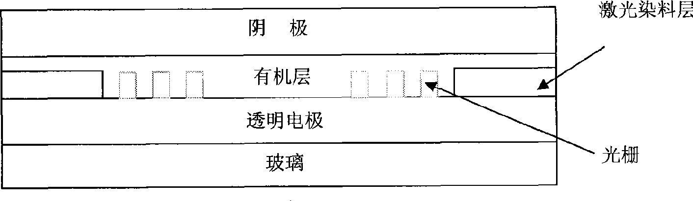
[0044] Embodiment one: see figure 1 . The thickness of the ITO is 150nm, the thickness of the organic layer is 250nm, and the thickness of the metal electrode layer is 200nm. The width of the middle active layer is 5mm. LiF was used as the DBR grating (refractive index 1.30) with a thickness of 150 nm. The grating has a diffraction order of 2.0 and a period of 360 nm. Coumarin6 was used as the material of the light-emitting layer, and DCM:AlQ (1.0% mass ratio) was used as the laser pigment layer (width 2.0 mm, thickness 150 nm). A pulse voltage is applied to the device with a pulse width (duration) of 5 microseconds and a period of 10 Hz. Thus realizing a red laser.

Embodiment 2

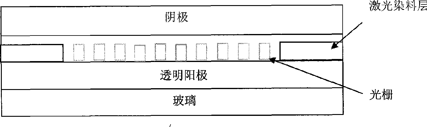
[0045] Embodiment two: see figure 2 . The thickness of the ITO is 150nm, the thickness of the organic layer is 250nm, and the thickness of the metal electrode layer is 200nm. A photoresist is used as the DFB grating with a thickness of 150nm. The grating has a diffraction order of 2.0 and a period of 200 nm. OXD7 was used as the material of the light-emitting layer, and DSB was doped in CBP as the laser pigment layer (width 2.0mm, thickness 150nm). A pulse voltage is applied to the device with a pulse width (duration) of 5 microseconds and a period of 10 Hz. Thus realizing a blue laser. Properties of the invented laser

[0046] First, the DCM2 thin film is pumped by laser, when the laser intensity reaches 3.9kw / cm 2 , the spectrum emitted by DCM2 will be narrowed, such as Figure 4 shown. Therefore, the purpose of this invention is to achieve high intensity EL light intensity, making it more than 3.9kw / cm 2 .

[0047] Through this invention, the intensity of cross-s...


PUM

PropertyMeasurementUnit
thicknessaaaaaaaaaa
refractive indexaaaaaaaaaa

Abstract

The invention relates to a novel organic semiconductor solid laser and a method for manufacturing thereof, wherein a distributing Bragg resonator DBR or a distributing feedback resonator DFB is arranged on the anode of an organic electroluminescent luminescent diode through adopting the photoetching technique, the resonator chooses LiF, SiO2, SiNx or Al2O3 to finish through a vacuum coating or a magnetron sputtering method, the calculation formula of Bragg wavelength lambda Bragg is that lambda Bragg=neff2 lambada / m, wherein neff is effective refractive index constant, m and lambada are respectively the diffraction order and the periodic time of grating. The novel organic semiconductor solid laser combines photoluminescence and electroluminescence, which utilizes EL light of high-intensity OLED and low ASE threshold organic thin film on the same device of a pump to avoid the organic luminescent layer in an OLED period from absorbing light by electric charge and exciton, avoid exciton resolution generated by strong light, and achieves OLED pump laser.

Description

technical field [0001] The invention relates to a novel organic semiconductor solid-state laser and a preparation method thereof. Background technique [0002] Organic solid-state laser is an important research direction in the research of organic solid-state semiconductor devices. Amplified spontaneous emission (ASE) has been observed for photopumped organic thin films or organic single crystals. However, so far, no scientific research group has reported the successful realization of organic electro-laser. According to the report of ASE phenomenon in photo-pumped organic laser dye thin films, the current density in the device should reach ~KA / cm2, which is the prerequisite for the realization of electro-laser. However, there is generally a problem of current efficiency drop, especially when a high voltage is applied, which restricts the improvement of the luminous power and external quantum efficiency of the device under high brightness conditions. It is generally believ...

Claims


Application Information

Patent Timeline
Patent Type & Authority Applications(China)
IPC IPC(8): H01S5/36H01S5/10
Inventor 魏斌孙三春张建华张志林
Owner SHANGHAI UNIV
Why Eureka
Try Eureka