Vertical channel organic field effect transistor and method for producing the same

A technology of vertical channels and organic fields, applied in the field of organic electronics, to achieve the effect of reducing difficulty, reducing cost and expanding the scope of application

Active Publication Date: 2009-04-08
INST OF MICROELECTRONICS CHINESE ACAD OF SCI
View PDF0 Cites 16 Cited by
  • Summary
  • Abstract
  • Description
  • Claims
  • Application Information

AI Technical Summary

Problems solved by technology

[0002] With the continuous deepening of information technology, electronic products have entered every link of people's life and work; in daily life, people's demand for low-cost, flexible, low-weight, and portable electronic products is increasing, while the traditional inorganic-based It is difficult for devices and circuits of semiconductor materials to meet these requirements, so organic microelectronics technology based on organic polymer semiconductor materials that can achieve these characteristics has received more and more attention under this trend

Method used


Image

  • Vertical channel organic field effect transistor and method for producing the same
  • Vertical channel organic field effect transistor and method for producing the same
  • Vertical channel organic field effect transistor and method for producing the same

Examples


Embodiment 1

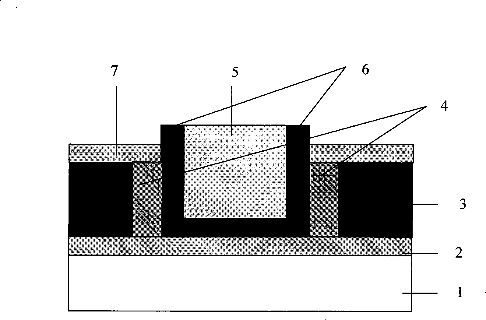
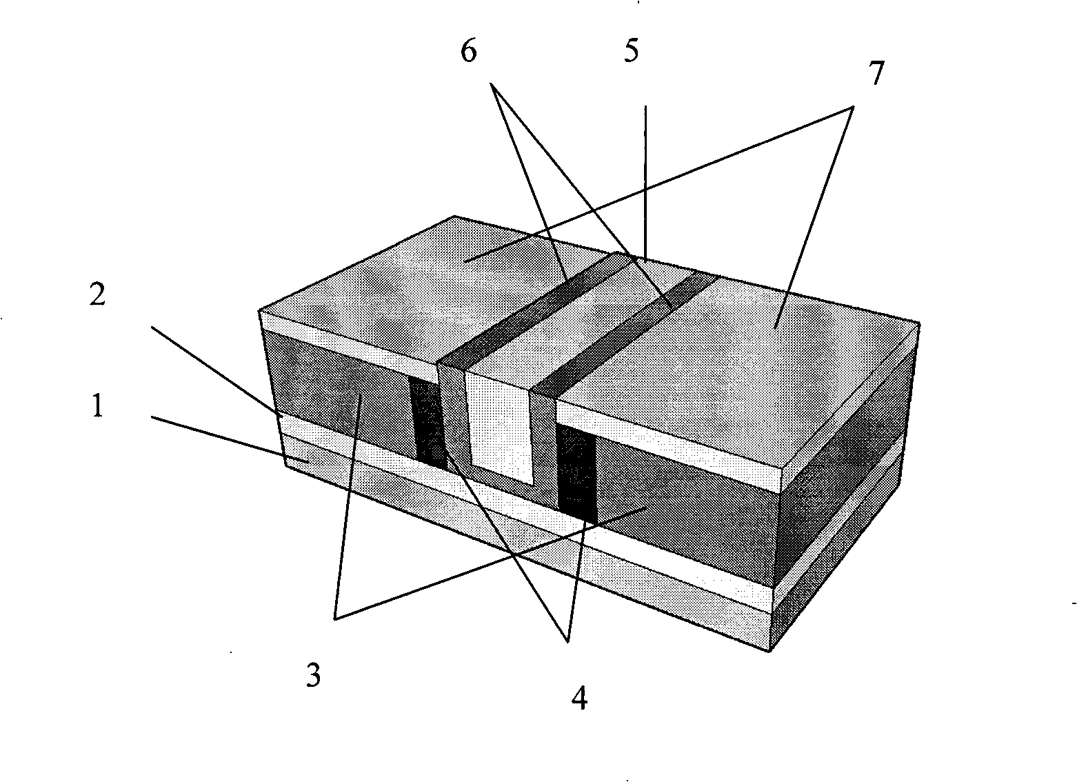
[0054] Depend on figure 1 As shown, the basic structure of the vertical channel organic field effect transistor of the present invention includes an insulating substrate, a metal gate electrode, a dielectric layer, an insulating layer for isolating source and drain electrodes, a vertical organic semiconductor layer, a planar metal source electrode and a planar metal drain electrode .

[0055] The insulating substrate is the base of this structure, and its manufacturing material is a silicon wafer with insulating films such as silicon oxide and silicon nitride, or insulating glass or insulating plastic film.

[0056] On the upper part of the insulating substrate is the source electrode, and the material of the source electrode can be a high-common function metal material such as gold, platinum or silver, or a conductive organic substance such as PEDOT:PSS. The source electrode is a planar electrode and is tiled on an insulating substrate.

[0057] The central part above the s...

Embodiment 2

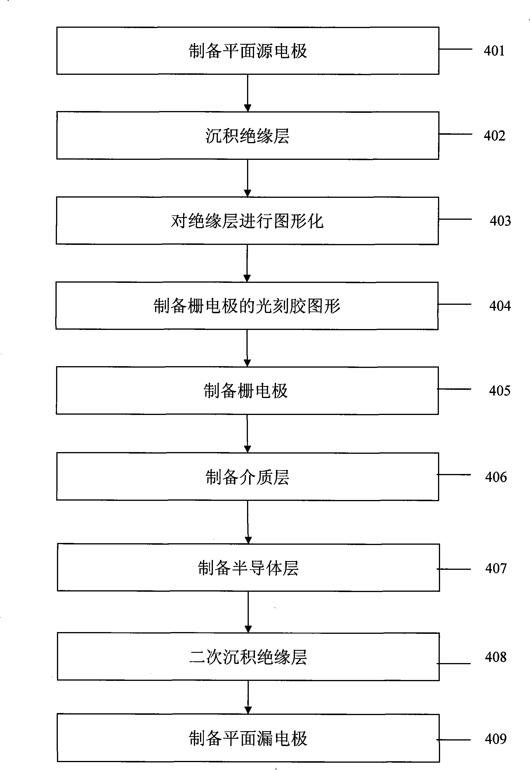
[0067] Such as image 3 As shown, the present invention also discloses a method for preparing a vertical channel organic field effect transistor, and its specific preparation steps are as follows:

[0068] see Figure 4 to Figure 12 .

[0069] Step 101: Prepare a planar gold source electrode on a thermally oxidized silicon insulating substrate. The specific preparation method of the planar source electrode used therein adopts the method of vacuum thermophysical deposition, electron beam deposition, sputtering metal electrode, ink-jet printing or spin-coating organic electrode.

[0070] Step 102: Deposit an insulating layer on the source electrode layer. The deposition method for the inorganic insulating layer is low-pressure chemical vapor deposition (LPCVD), sputtering or atomic layer deposition (ALD), etc.; the deposition method for the organic insulating layer is spin coating or inkjet printing. In this embodiment, an electron beam evaporation deposition method is used ...


PUM


Abstract

The invention discloses a vertical channel organic field effect transistor, and belongs to the field of organic microelectronics. The structure of the vertical channel organic field effect transistor comprises a metal source electrode at an insulating substrate, a gate dielectric layer, an insulating layer, an organic semiconductor layer, a gate electrode and a metal drain electrode, wherein, the long strip-shaped gate electrode is surrounded at the exact center of the device by the dielectric layer and the organic semiconductor material; both the source electrode and the drain electrode are planar electrodes, and by changing the direction of the channel from horizontal direction to vertical direction, the length of the channel can be effectively controlled only by controlling the growth thickness of a thin film, thus avoiding the expensive electron beam lithography, and providing a simple and convenient and low-cost method for preparing a short-channel organic field effect transistor. A method for preparing the vertical channel organic field effect transistor is also provided.

Description

technical field [0001] The invention relates to the field of organic electronics, in particular to a vertical channel organic field effect transistor and a preparation method thereof. Background technique [0002] With the continuous deepening of information technology, electronic products have entered every link of people's life and work; in daily life, people's demand for low-cost, flexible, low-weight, and portable electronic products is increasing, while the traditional inorganic-based It is difficult for devices and circuits of semiconductor materials to meet these requirements, so organic microelectronics technology based on organic polymer semiconductor materials that can achieve these characteristics has received more and more attention under this trend. [0003] Organic field effect transistors are the basic components of organic circuits, and their performance plays a decisive role in the performance of the circuit. Among them, the mobility determines the speed of...

Claims


Application Information

Patent Timeline
Patent Type & Authority Applications(China)
IPC IPC(8): H01L51/05H01L51/10H01L51/40
Inventor 商立伟刘明涂德钰刘舸刘兴华
Owner INST OF MICROELECTRONICS CHINESE ACAD OF SCI
Why Eureka
Try Eureka