Miniature atomic air chamber encapsulation apparatus and technology method
An atomic gas chamber and packaging process technology, applied in microstructure technology, welding equipment, opto-mechanical equipment, etc., can solve the problems of mass production difficulty, low production efficiency, and light loss of ordinary glass blowing technology
- Summary
- Abstract
- Description
- Claims
- Application Information
AI Technical Summary
Problems solved by technology
Method used
Image
Examples
Embodiment 1
[0079] The following embodiments describe in detail the components and design parameters of the miniature gas chamber packaging device.
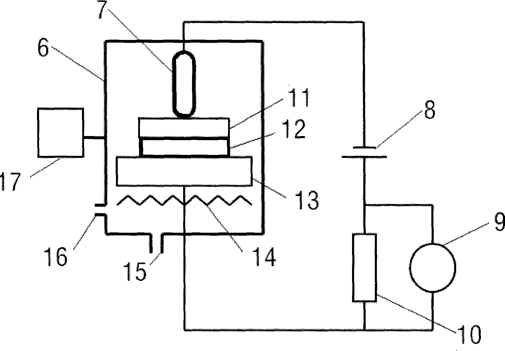
[0080] This equipment is mainly composed of sample chamber (ie vacuum chamber), vacuum unit, heating and temperature control device, DC high voltage device, air intake device and bonding process monitoring device. like Image 6 As shown, the connection relationship is: the vacuum chamber is connected with the vacuum unit and the air intake device, the latter is used to evacuate or inflate the vacuum chamber; the heating and temperature control device includes the heating wire and temperature measuring probe in the vacuum chamber, and the vacuum chamber and the The temperature control instrument connected to it; the DC high-voltage device includes an insulating indenter and a grounded sample stage in the vacuum chamber, and a DC high-voltage power supply connected to it outside the vacuum chamber; the bonding process monitoring device is conn...
Embodiment 2
[0090] The following examples illustrate in detail that by using the equipment described in the first example above, an inert gas of a certain pressure (such as helium, argon or neon) can be sealed in a micro-gas chamber with a three-layer structure of "glass-perforated silicon wafer-glass". , and ensure that its leak rate is small enough. Proceed as follows:
[0091] First, material selection and preparation: In the above-mentioned three-layer structure of "glass-perforated silicon wafer-glass", the glass sheets on both sides are made of Pyrex heat-resistant glass (thickness 0.2mm-0.5mm) rich in alkali metal oxides, and the middle The samples are double-sided polished P-type single crystal silicon wafers (thickness 0.5mm-5mm). Both the glass and the silicon wafer are cut into small pieces by photolithography, and the size of the silicon wafer is 15mm×15mm; the size of the glass is 8mm×8mm and 20mm×10mm, which are used to package the first side and the second side of the per...
Embodiment 3
[0098] The following examples describe in detail, using the equipment described in Example 1 above and the double-sided bonding packaging process described in Example 2, using the in-situ chemical reaction method of barium azide and rubidium chloride to realize the "glass-drilling" The process of encapsulating metal rubidium in a micro-gas chamber with a three-layer silicon wafer-glass structure. Proceed as follows:
[0099] First, the implementation steps of material selection and preparation, sample cleaning, and first-side bonding are exactly the same as the process steps corresponding to the second embodiment above.
[0100] Second, according to the chemical reaction (BaN 6 +2RbCl→BaCl 2 +3N 2 ↑+2Rb↑) The mass ratio of the balance formula, weigh a certain amount of barium azide (BaN 6 ) and rubidium chloride (RbCl). After the two are mixed, they are added to an appropriate amount of deionized water to form a solution. The reaction mixture is obtained after baking to ...
PUM
| Property | Measurement | Unit |
|---|---|---|
| thickness | aaaaa | aaaaa |
| thickness | aaaaa | aaaaa |
| surface roughness | aaaaa | aaaaa |
Abstract
Description
Claims
Application Information


