Substrate for flexible organic optoelectronic device and preparation method thereof

A technology for optoelectronic devices and substrates, which is applied in the fields of electric solid-state devices, semiconductor/solid-state device manufacturing, photovoltaic power generation, etc., can solve problems such as poor adhesion between thin films and substrates, reduce production costs and process difficulties, achieve optimal results, and improve performance effect

Inactive Publication Date: 2009-06-24
UNIV OF ELECTRONICS SCI & TECH OF CHINA
View PDF0 Cites 38 Cited by
  • Summary
  • Abstract
  • Description
  • Claims
  • Application Information

AI Technical Summary

Problems solved by technology

[0007] The technical problem to be solved by the present invention is how to provide a substrate for flexible organic optoelectronic devices and its preparation method, which solves the problem of poor adhesion between the deposited film and the substrate due to the low surface energy of the flexible substrate, and improves the The barrier performance of the substrate to water and oxygen, and at the same time play a good smoothing effect on the surface of the substrate

Method used


Image

  • Substrate for flexible organic optoelectronic device and preparation method thereof
  • Substrate for flexible organic optoelectronic device and preparation method thereof
  • Substrate for flexible organic optoelectronic device and preparation method thereof

Examples


Embodiment 1

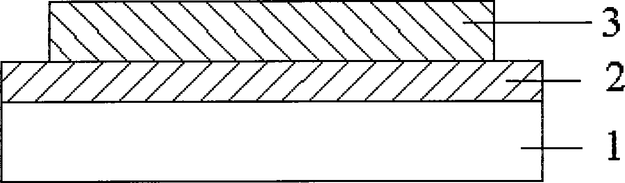
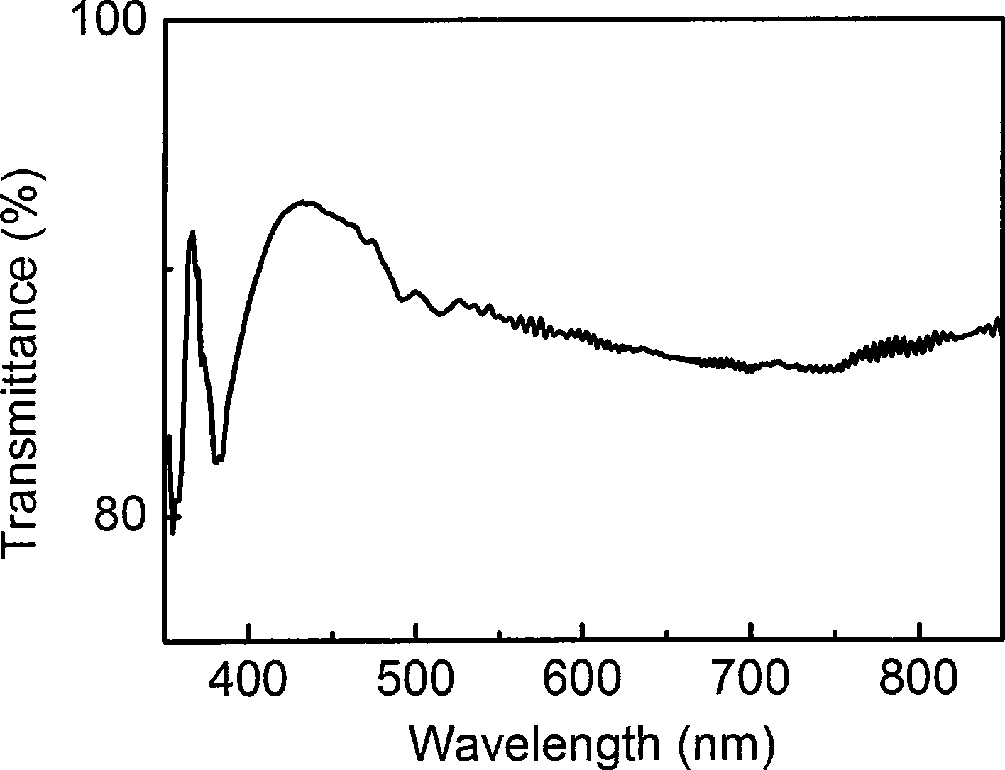
[0105] like figure 1 In the substrate structure shown, the flexible substrate 1 is a flexible polyethylene terephthalate polymer (PET) substrate, the bonding layer 2 is a single-layer UV-curable adhesive, and the conductive film 3 is ITO sputtered by DC magnetron. Transparent conductive film. The transmittance test curve is as figure 2 shown.

[0106] The preparation method is as follows:

[0107] ①Use detergent, acetone solution, ethanol solution and deionized water to ultrasonically clean the PET substrate, and dry it with dry nitrogen after cleaning;

[0108] ② Stir the UV-curable adhesive diluted 1:10 with ethanol for 20 hours, then spin-coat it on the PET surface at a speed of 2000 rpm for one minute, and the film thickness is about 100 nanometers;

[0109] ③UV curing treatment on the surface of the substrate for 30 seconds;

[0110] ④Put the substrate into a vacuum chamber, and at room temperature, by means of DC magnetron sputtering, sputter a 100-nm thick ITO tra...

Embodiment 2

[0114] like figure 1 In the substrate structure shown, the flexible substrate 1 is made of a flexible metal foil, the adhesive layer 2 is made of a single-layer UV-curable adhesive, and the conductive film 3 is a DC magnetron sputtered ITO transparent conductive film.

[0115] The preparation method is as follows:

[0116] ①Use detergent, acetone solution, ethanol solution and deionized water to ultrasonically clean the flexible metal foil, and dry it with dry nitrogen after cleaning;

[0117] ② Stir the UV-curable adhesive diluted 1:1 with ethanol for 30 hours, then spin-coat it on the surface of the flexible metal foil at a speed of 3000 rpm for 1 minute, and the film thickness is about 200 nanometers;

[0118] ③UV curing treatment on the surface of the substrate for 30 seconds;

[0119] ④ Put the substrate into the vacuum chamber, and at room temperature, by means of DC magnetron sputtering, sputter a 200-nm thick ITO transparent conductive film on the surface of the flex...

Embodiment 3

[0122] like figure 1 In the substrate structure shown, the flexible substrate 1 is a PET substrate, the bonding layer 2 is a single-layer UV-curable adhesive, and the conductive film 3 is a metal conductive film prepared by thermal evaporation.

[0123] ①Use detergent, acetone solution, ethanol solution and deionized water to ultrasonically clean the surface of the PET substrate, and dry it with dry nitrogen after cleaning;

[0124] ② Stir the UV-curable adhesive diluted 1:10 with ethanol for 20 hours, then spin-coat it on the PET surface at a speed of 2000 rpm for one minute, and the film thickness is about 100 nanometers;

[0125] ③Irradiate the surface of the substrate with ultraviolet light for 30 seconds;

[0126] ④Put the substrate into a vacuum chamber, and evaporate a 100nm thick metal conductive film on the surface of the PET substrate by thermal evaporation at room temperature;

[0127] ⑤After taking the substrate out of the vacuum chamber, irradiate with ultraviol...


PUM


Abstract

The invention discloses a flexible substrate used for optoelectronic devices and comprises a flexible substrate; the invention is characterized in that a bonding layer and a conductive thin film are arranged on the surface of the flexible substrate; the conductive thin film is deposited on the surface of the bonding layer; the bonding layer is made of UV-curable adhesive; and the adhesive is the mixture of free radical type UV-curable adhesive and cationic type UV-curable adhesive. The cationic-type and free radical-type UV-curable adhesives are united in one to make full use of light energy and achieve mutual modification; the curing product concentrates the advantages of epoxy resin and acrylic resin and overcomes certain shortcomings, thereby creating a brand-new system.

Description

technical field [0001] The invention relates to the technical field of organic optoelectronic devices, in particular to a flexible organic optoelectronic device substrate and a preparation method thereof. Background technique [0002] Optoelectronics technology is a high-tech industry that develops rapidly after microelectronics technology. With the rapid development of optoelectronic technology, optoelectronic products such as solar cells, optical image sensors, plasma flat panel displays, electroluminescent displays, thin film transistors, and liquid crystal display panels have gradually matured, and they have greatly improved human life. At the same time, the wide application of optoelectronic information technology in various fields of social life has also created a huge growing market. Developed countries regard the optoelectronic information industry as one of the key development areas, and the competition in the optoelectronic information field is unfolding worldwide...

Claims


Application Information

Patent Timeline
Patent Type & Authority Applications(China)
IPC IPC(8): H01L51/00H01L51/44H01L51/46H01L51/48H01L51/52H01L51/54H01L51/56C09J167/06C09J4/00C09J163/00
CPCY02E10/50Y02E10/549
Inventor 于军胜李璐蒋亚东王娜娜
Owner UNIV OF ELECTRONICS SCI & TECH OF CHINA
Why Eureka
Try Eureka