Method for preparing super-hydrophobic antireflex micron and nano composite structure surface

A nano-composite and super-hydrophobic technology, applied in the direction of silicon, can solve the problems of expensive instruments, restricted applications, and limited applications, and achieve the effects of low cost, reduced pressure loss along the process, and strong universality

Inactive Publication Date: 2009-07-08
JILIN UNIV
View PDF0 Cites 60 Cited by
  • Summary
  • Abstract
  • Description
  • Claims
  • Application Information

AI Technical Summary

Problems solved by technology

Although the method of electron beam etching has the advantages of high precision and high resolution, its wide application is restricted due to the disadvantages of expensive equipment and low efficiency.
Based on the structure prepared by the self-assembled nanoparticle method, laser interference etching and nanoimprinting mask, RIE can construct a sub-wavelength structure with anti-reflection properties on a large area (Nanotechnology 2000.11.161; Nanotechnology 1997.8.53 ; AppI.Phys.Lett.2002.80.2242; J.Vac.Sci.Tehchnol.2003.21.287 4Small 2008.4.1972 Chinese patent, publication number CN1378581A, CN1613565 A, CN1624062 A), but the instruments required by these techniques are still very expensive, make its application severely limited

Method used


Image

  • Method for preparing super-hydrophobic antireflex micron and nano composite structure surface
  • Method for preparing super-hydrophobic antireflex micron and nano composite structure surface
  • Method for preparing super-hydrophobic antireflex micron and nano composite structure surface

Examples


Embodiment 1

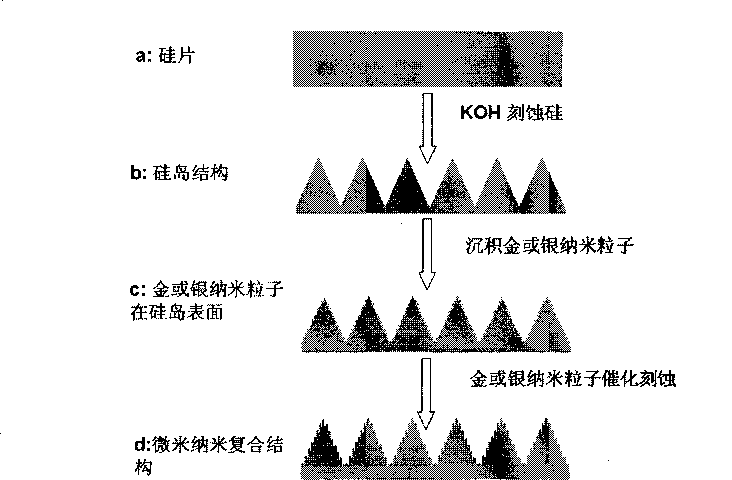
[0045] (1) Select n-100 type silicon wafer and clean its surface. The treatment process is as follows: ultrasonically clean the silicon wafer in acetone, chloroform, ethanol, and water respectively, with an ultrasonic power of 100W for 5 minutes. Then put the silicon chip into the HF solution with a mass fraction of 1% for 5 minutes to remove the silicon dioxide on the surface, and finally wash it with deionized water and dry it with high-purity nitrogen gas.

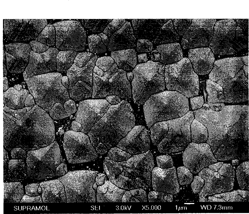
[0046] (2) Prepare micron-scale silicon island structures on the silicon surface. The process is as follows: put the cleaned silicon wafer into a KOH solution at 60°C with a pH of 14 for 1 hour, and silicon is etched anisotropically in the alkaline solution. , thereby preparing a silicon island structure on the silicon surface, the bottom side of the silicon island is 4-6 μm long, and the height is 5-7 μm. like figure 2 shown.

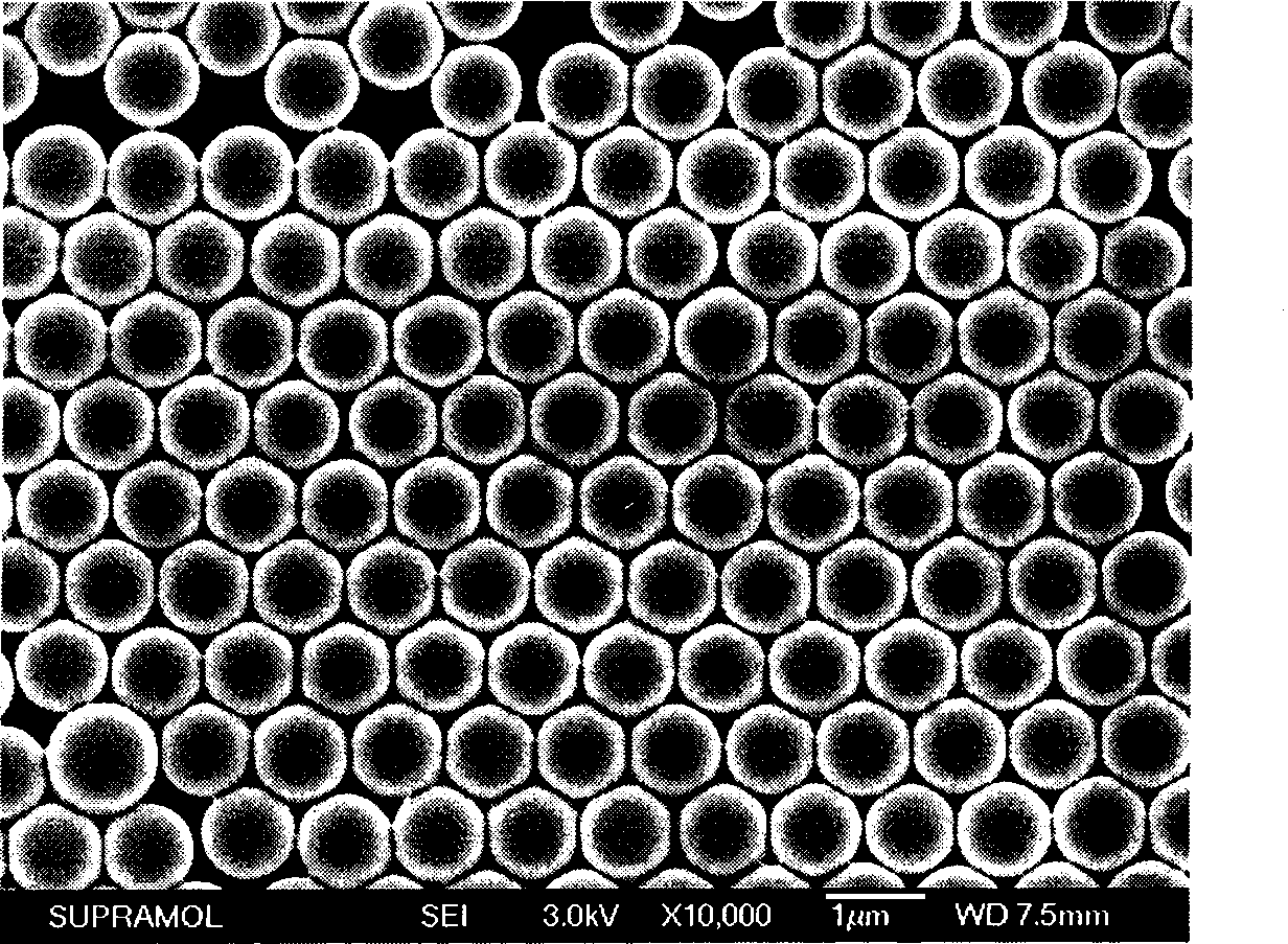
[0047] (3) To prepare nanoscale pores on the surface of micron-scale silicon islands, fi...

Embodiment 2

[0050] According to the method and steps of Example 1, the electroless deposition of silver nanoparticles is changed to electrodeposition, and the electrolyte is AgNO of 0.01M. 3 Solution, deposition voltage is 400mv, deposition time is 15min, other steps are the same as embodiment 1, superhydrophobic anti-reflection silicon surface can be obtained equally, the silicon island height of preparation structure is 5~7 μ m, the size of nanoscale hole is about 130 nanometers, The contact angle is 153°, and the reflectance is lower than 8%.

Embodiment 3

[0052] According to the method and steps of Example 1, the electroless deposition of silver nanoparticles is changed to electrodeposition of gold nanoparticles, the electrolyte is 0.01M chloroauric acid solution, the deposition voltage is 500mv, and the deposition time is 10min. Other steps are the same as in the embodiment. 1. The superhydrophobic anti-reflective silicon surface can also be obtained. The height of the silicon island of the prepared structure is 5-7 μm, the size of the nanoscale hole is about 120 nanometers, the contact angle is 150°, and the reflectivity is lower than 8%.


PUM

PropertyMeasurementUnit
thicknessaaaaaaaaaa
heightaaaaaaaaaa
heightaaaaaaaaaa

Abstract

The invention belongs to the technical field of preparing the surface of a composite structure, and in particular relates to a method for preparing super-hydrophobic antireflective silicon surface with a micron and nanometer composite structure. The method comprises the following steps: cleaning a silicon chip; preparing a micron-level silicon island and a gridding structure on the surface of the silicon chip; carrying out catalytic etching taking silver or aurum nanoparticles as blockage; obtaining the surface of the micron and nanometer composite structure; and carrying out chemical modification of the surface of the composite structure. A static contact angle between the super-hydrophobic antireflective material surface prepared by the method and water is more than 150 degrees, and a static rolling angle of water is less than 3 degrees. The surface has superior antireflective performance, and in particular, the light reflectivity within the wavelength range between 800 and 1,100 nm is less than 3 percent. With application of the method, the super-hydrophobic antireflective silicon surface of the micron and nanometer composite structure can be produced on scale, can be widely applied to a solar cell, a microfluidic chip, a photoelectric device, and the like, and has good industrial application prospect.

Description

technical field [0001] The invention belongs to the technical field of preparation of composite structure surfaces, and in particular relates to a method for preparing superhydrophobic anti-reflection silicon surfaces of micron and nanometer composite structures. Background technique [0002] In recent years, countries all over the world have given great enthusiasm and attention to MEMS. It is becoming a new large-scale industry, a new growth point of the national economy, and has a significant impact on the development of national defense technology. However, with the miniaturization of devices and systems, the feature scale decreases, and the surface area (L 2 ) and volume (L 3 ) ratio is also relatively increased, the surface effect is enhanced, and the surface force that has been neglected in the macro scale now plays a dominant role, resulting in a series of problems such as surface friction, wear, adhesion and pressure loss, making (MEMS) devices was greatly troubled...

Claims


Application Information

Patent Timeline
Patent Type & Authority Applications(China)
IPC IPC(8): C01B33/02
Inventor 吕男齐殿鹏徐洪波黄春玉高立国迟力峰
Owner JILIN UNIV
Why Eureka
Try Eureka