Enhanced AlGaN/GaN field effect tube and manufacturing method thereof

A fabrication method and technology for field effect transistors, which are applied in semiconductor/solid-state device manufacturing, electrical components, circuits, etc., can solve problems such as deteriorating device performance and reliability, and achieve a simple and reliable implementation method, reduce complexity, and reduce sources of energy. The effect of leakage access resistance

Active Publication Date: 2009-07-08
SUN YAT SEN UNIV
View PDF0 Cites 11 Cited by
  • Summary
  • Abstract
  • Description
  • Claims
  • Application Information

AI Technical Summary

Problems solved by technology

As the mainstream technology, recessed gate structure and gate fluoride plasma implantation, due to the use of plasma etching and implantation methods, will inevitably cause material damage, thereby deteriorating the working performance and reliability of the device

Method used


Image

  • Enhanced AlGaN/GaN field effect tube and manufacturing method thereof
  • Enhanced AlGaN/GaN field effect tube and manufacturing method thereof
  • Enhanced AlGaN/GaN field effect tube and manufacturing method thereof

Examples


Embodiment 1

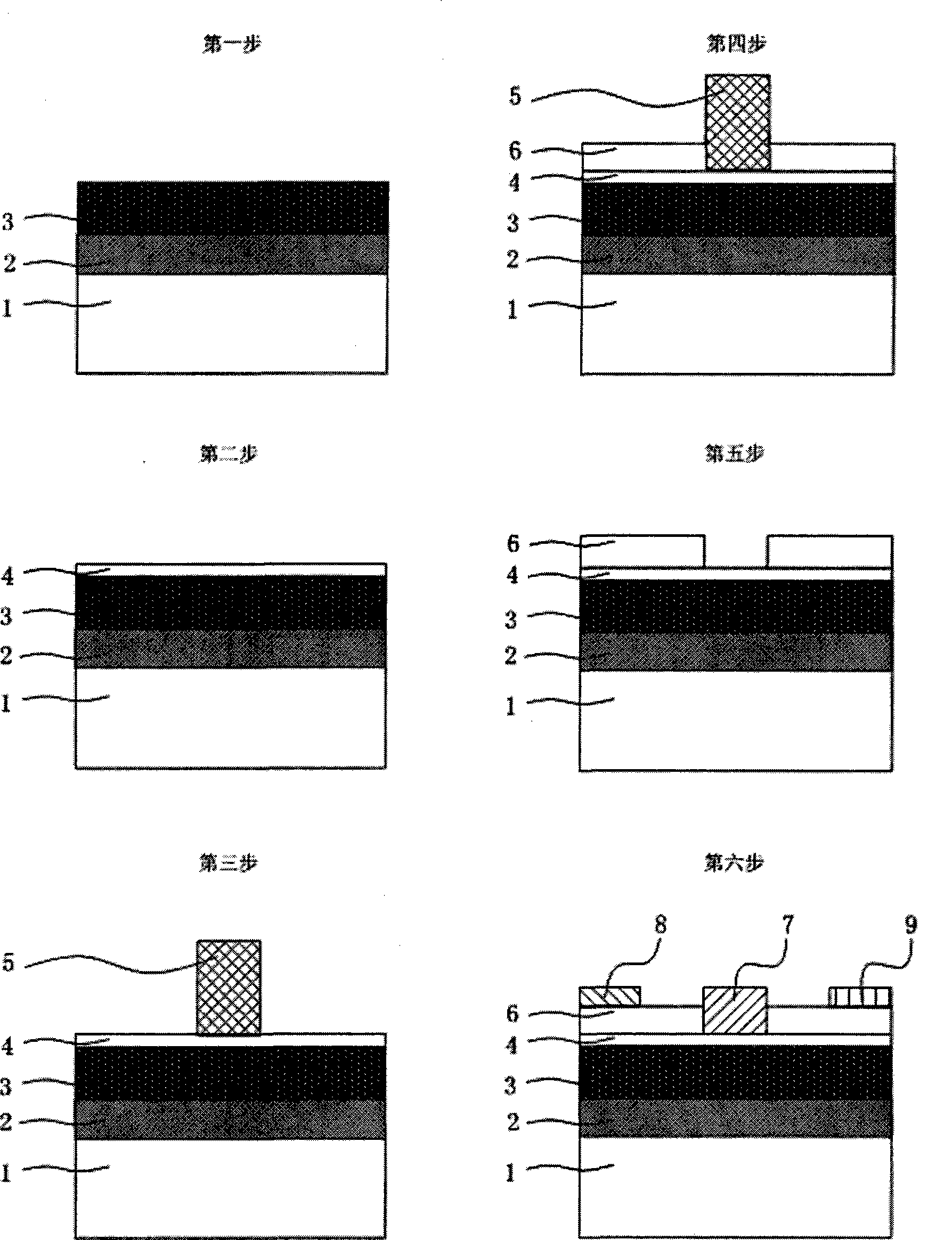
[0033] Such as image 3 As shown, the present invention provides a method for manufacturing an enhanced AlGaN / GaN field effect transistor, which includes the following steps:

[0034] Step 1: Using a 300 μm thick sapphire (Sapphire) substrate 1, using the MOCVD method, at a temperature of 1100 ° C, hydrogen and ammonia as protective gases, first grow a 20 nm thick AlN buffer layer 2, and then control the growth conditions A high-resistance GaN layer 3 with a thickness of 3 μm is grown thereon.

[0035] Step 2: Using the MOCVD method to maintain a growth temperature of about 1100° C., and controlling the flows of the aluminum source and the gallium source fed into the reaction chamber, grow an AlGaN thin layer 4 with a thickness of 5-10 nm. The AlGaN layer and the GaN layer 3 have different compositions. A low-concentration two-dimensional electron gas is formed at the interface.

[0036] Step 3: On the AlGaN thin layer 4 with a thickness of 5-10nm, first deposit SiO with a t...

Embodiment 2

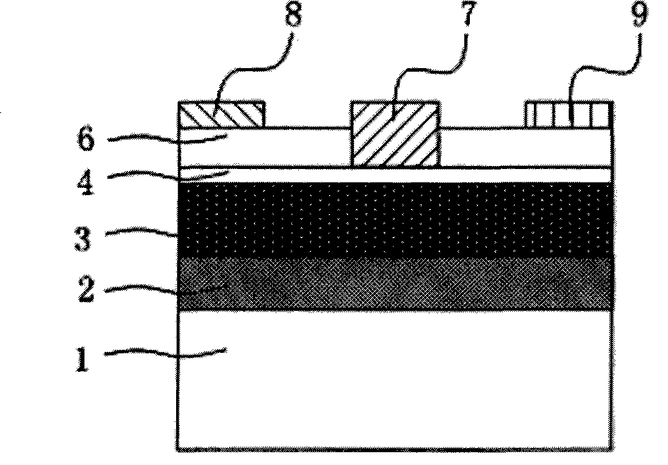
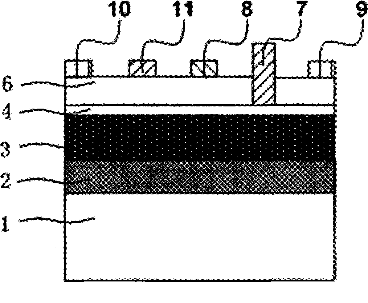
[0045] Such as figure 2 As shown, this embodiment adopts the same steps as Step 1 to Step 6 in Embodiment 1. Then, on the secondary grown second AlGaN layer 6 , continue to use the vapor deposition method to form the Ti / Al / Ni / Au second drain 10 first, and then form the Ni / Au second gate 11 . In this way, the gate electrode 7 on the first AlGaN layer 4 grown once and the source electrode 8 and drain electrode 9 on the second AlGaN layer 6 grown secondarily constitute a local enhanced AlGaN / GaN HFET structure; On the grown second AlGaN layer 6, a local depletion-type AlGaN / GaN HFET structure is formed by the source 8, the drain 10, and the gate 11, thereby forming a composite AlGaN / GaN HFET in which enhancement and depletion coexist. structure.


PUM


Abstract

The invention relates to a method for manufacturing an enhanced type AlGaN/GaN/ field effect transistor, namely a method for manufacturing AlGaN/GaN HFET by adopting a secondary growth AlGaN layer. The method comprises the following steps: firstly, a buffer layer grows on a substrate firstly, and a GaN epitaxial layer grows on the buffer layer; secondly, a first AlGaN layer grows on the GaN epitaxial layer to accomplish the first material growth; thirdly, a SiO2 mask membrane is deposited on the first AlGaN layer, and the SiO2 mask membrane formed on a grid zone is reserved through the photoetching method; fourthly, a second AlGaN layer grows on the unmasked first AlGaN layer to accomplish the second material growth; fifthly, the SiO2 mask membrane is removed; sixthly, a source electrode and a drain electrode are formed on the second AlGaN layer, and then a grid electrode is formed on the grid zone. Moreover, the invention also discloses the enhanced type AlGaN/GaN/ field effect transistor. The method has the advantages of simple process and good reliability, and can obtain higher threshold voltage and transconductance.

Description

technical field [0001] The invention relates to the field of GaN-based microwave and power devices, in particular to an enhanced AlGaN / GaN field effect transistor and a manufacturing method thereof. Background technique [0002] Compared with traditional III-V semiconductor materials, GaN-based materials have obvious characteristics such as shorter bond lengths and larger forbidden band widths. Short bond length means large bond energy and small atomic mass, resulting in large phonon energy, and lattice scattering is difficult to occur, which will result in high thermal conductivity and saturation mobility at the macroscopic level. The large forbidden band width makes the breakdown electric field higher, and the avalanche effect is difficult to occur. At the same time, the generation of intrinsic carriers and leakage current at high temperature is reduced. When AlGaN and GaN form a heterojunction, due to the strong spontaneous polarization of the two nitrides and the piezo...

Claims


Application Information

Patent Timeline
Patent Type & Authority Applications(China)
IPC IPC(8): H01L21/335H01L29/778
Inventor 刘扬江灏文于华张佰君王钢
Owner SUN YAT SEN UNIV
Why Eureka
Try Eureka