Method for manufacturing aluminum nitride silicon tip and grids structure

A manufacturing method and technology of aluminum nitride, applied in chemical instruments and methods, cleaning methods using liquids, cleaning methods and utensils, etc., can solve the problem of poor consistency and controllability of aluminum nitride cones, low success rate, and adhesion Inadequate problems, achieve stable electrical and thermal performance, overcome poor angle and height consistency

Active Publication Date: 2009-08-05
INST OF PHYSICS - CHINESE ACAD OF SCI
View PDF0 Cites 10 Cited by
  • Summary
  • Abstract
  • Description
  • Claims
  • Application Information

AI Technical Summary

Problems solved by technology

[0008] One of the objectives of the present invention: not only to overcome the disadvantages of poor consistency and controllability, low success rate and poor adhesion of aluminum nitride cones prepared by chemical vapor deposition, but also to overcome the disadvantages of forming cone structures by plasma etching process Angle and height consistency is very poor, the ratio of length to diameter is relatively small, and the radius of curvature of the top is relatively large; thus providing a method of using focused ion beam etching to prepare a high aspect ratio, small tip radius, and controllable density. The method of aluminum nitride nano-cones, which has the advantages of less preparation steps, simple process, good repeatability, etc.
[0009] The second object of the present invention is to provide a method for directly fabricating a gate aluminum nitride cone field emission structure on an aluminum nitride film coated with a gold film by using focused ion beam etching technology, which overcomes the traditional Spindt type The shortcomings of complex manufacturing process and low efficiency of field emission structure

Method used


Image

  • Method for manufacturing aluminum nitride silicon tip and grids structure
  • Method for manufacturing aluminum nitride silicon tip and grids structure
  • Method for manufacturing aluminum nitride silicon tip and grids structure

Examples


Embodiment 1

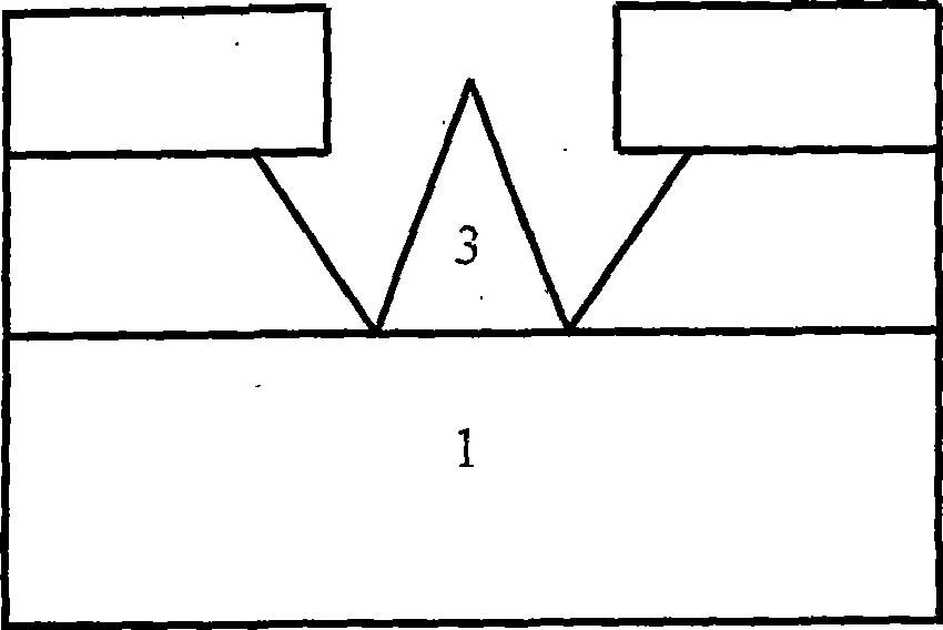
[0040] The aluminum nitride cone tip structure of this embodiment is shown in Figure 4(a); the prepared aluminum nitride cone tip has an aspect ratio of ~5, a tip curvature radius of ~150 nanometers, and a bottom diameter of ~1 micron. Its detailed process flow is as follows:

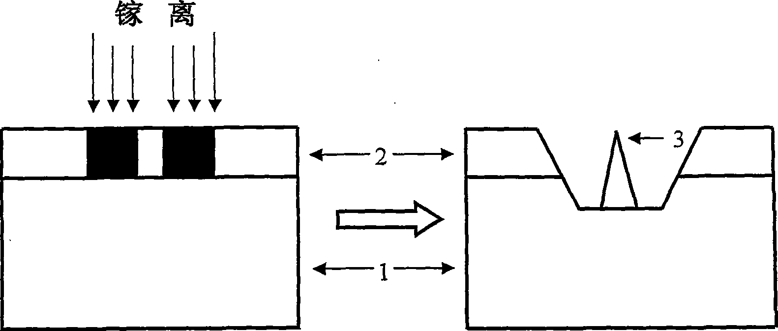
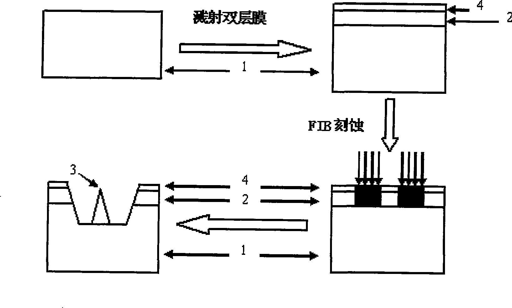
[0041] 1) Take a piece of (001) oriented monocrystalline silicon as the substrate 1, adopt a conventional semiconductor cleaning process, and ultrasonically clean it in acetone, alcohol and deionized water in sequence, and dry it with nitrogen gas after cleaning, and set it aside;

[0042] 2) On the silicon substrate 1 obtained by cleaning in step 1), put it into a radio frequency magnetron sputtering system, and grow a layer of aluminum nitride film 2 by radio frequency magnetron sputtering method, and the growth conditions are as follows: nitrogen / argon The mixing ratio is 17.5:10.2, the growth temperature is 700oC, the sputtering pressure is 15mTorr, the sputtering incident power is 100W, the reflect...

Embodiment 2

[0045] The aluminum nitride cone tip structure of this embodiment is shown in FIG. 4( b ); the prepared aluminum nitride cone tip has an aspect ratio of ~8, a tip curvature radius of ~50 nm, and a bottom diameter of ~0.6 μm. Its detailed process flow is as follows:

[0046] 1) Take a piece of (001) oriented single crystal silicon as the substrate 1, adopt a conventional semiconductor cleaning process, ultrasonically clean it in acetone, alcohol and deionized water in sequence, and then dry it with nitrogen;

[0047] 2) On the silicon substrate 1 obtained by cleaning in step 1), put it into a radio frequency magnetron sputtering system, and grow a layer of aluminum nitride film 2 by radio frequency magnetron sputtering method, and the growth conditions are as follows: nitrogen / argon The mixing ratio is 17.5:10.2, the growth temperature is 700 degrees Celsius, the sputtering pressure is 15mTorr, the sputtering incident power is 100W, the reflected power is 0.5W, the sputtering t...

Embodiment 3

[0050] The aluminum nitride cone tip structure of this embodiment is shown in FIG. 4( c ): the aluminum nitride cone tip 3 has an aspect ratio of ~16, a tip curvature radius of about 20 nm, and a bottom diameter of ~0.4 μm. The specific preparation steps are as follows:

[0051] 1) Take a piece of (001) oriented single crystal silicon as the substrate 1, adopt a conventional semiconductor cleaning process, ultrasonically clean it in acetone, alcohol and deionized aqueous solution in sequence, and then dry it with nitrogen;

[0052] 2) On the silicon substrate 1 obtained by cleaning in step 1), a layer of aluminum nitride film 2 is grown by radio frequency magnetron sputtering method, and the growth conditions are as follows: the ratio of nitrogen / argon gas mixture is 17.5:10.2, the growth temperature The temperature is 700oC, the sputtering pressure is 15mTorr, the sputtering incident power is 100W, the reflected power is 0.5W, the sputtering time is 3 hours, and the (002)-ori...


PUM

PropertyMeasurementUnit
thicknessaaaaaaaaaa
diameteraaaaaaaaaa
radiusaaaaaaaaaa

Abstract

The invention relates to a preparation method of an aluminum nitride conical tip and a grid conical tip structure thereof. The method comprises the following steps: a layer of aluminum nitride film grows on a clean silicon substrate or a layer of gold film is then deposited on the clean silicon substrate by a radio-frequency magnetic control sputtering method; the silicon substrate is then put in a focused ion beam etching system; when the vacuum degree reaches 5.5 multiplied by 5-10mbar, a 5kV electron beam high voltage is applied to observe and position the appearance of a sample; an ion beam source is applied, and a beam current is arranged; finally, an etching pattern is arranged finally, and the focused ion beam etching is implemented to the aluminum nitride film sample according to the etching pattern to obtain the aluminum nitride conical tip 3 structure or the grid conical tip structure. The length-diameter ratio of a single cone of the aluminum nitride conical tip 3 structure is between (3-30):1, the minimum curvature radius of the tip part is less than 20 nanometer, and the diameter at the bottom is 100 nanometer to few microns. The invention can prepare the aluminum nitride conical tip and the grid conical tip structure thereof with controllable length-diameter ratio, omits a plurality of working procedures of depositing an insulating layer, photoetching, and the like which are necessary in the traditional process and has simple process and low cost.

Description

technical field [0001] The invention relates to an aluminum nitride cone tip material and a manufacturing method thereof, in particular to a nitrogen alloy with a high aspect ratio and a small radius of curvature of the tip, and a controllable aspect ratio and a controllable shape. The manufacture method of the aluminum nitride cone tip, and the manufacture method of the aluminum nitride cone tip field emission structure with the spindt structure are constructed on this basis. Background technique [0002] Aluminum nitride has become an important field emission cold cathode material because of its negative electron affinity, good chemical stability and thermal stability. Usually, the main factors that determine the emission characteristics of field emission materials include the work function of the material itself and the geometric shape of the material. For nanomaterials, the common geometric shapes such as nanotubes, nanowires or rods and nanocones are all due to their sm...

Claims


Application Information

Patent Timeline
Patent Type & Authority Applications(China)
IPC IPC(8): C23C14/35C23C14/02B08B3/12C23C14/06C23C14/14C23C14/54
Inventor 顾长志李云龙李俊杰时成瑛金爱子罗强杨海方
Owner INST OF PHYSICS - CHINESE ACAD OF SCI
Why Eureka
Try Eureka