Thinning corrosion method for heavily-doped stibium silicon chip

A technology of heavily doped antimony silicon wafers, which is applied in the fields of electrical components, semiconductor/solid-state device manufacturing, circuits, etc., can solve problems such as irremovable, chromium heavy metal pollution, damage to device electrical performance and long-term reliability, etc., and achieve silicon wafer The surface is smooth and consistent, avoiding metal pollution, and good ohmic contact effect

Inactive Publication Date: 2009-08-26
深圳深爱半导体股份有限公司
View PDF0 Cites 6 Cited by
  • Summary
  • Abstract
  • Description
  • Claims
  • Application Information

AI Technical Summary

Problems solved by technology

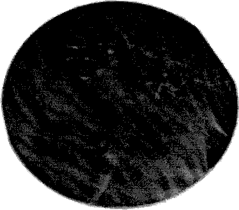
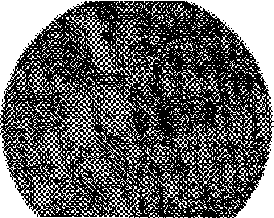
However, when etched with conventional acidic etchants (HF acid and HNO3), irregular white marks are formed on the surface (see figure 1 ), these white marks are mainly generated by the combined action of nitric acid vapor and decomposition gas in a short period of time when the silicon wafer enters the nitric acid, and these white marks cannot be removed by conventional methods unless the silicon wafer is re-grinded. It will appear again when it enters the corrosive solution, and the white imprint cannot achieve good ohmic contact at all. figure 2 shown
Another solution is to use alkaline etching solution for thinning and etching. However, as a semiconductor production line, it is taboo to introduce alkali metal ions, because alkali metal ions are highly mobile in semiconductor materials. In-chip movement, seriously impairing device electrical performance and long-term reliability
There are also hexavalent chromium combined with HF acid for thinning corrosion treatment, but the oxidation reaction speed of hexavalent chromium is too slow, and it also causes heavy metal pollution of chromium

Method used


Image

  • Thinning corrosion method for heavily-doped stibium silicon chip
  • Thinning corrosion method for heavily-doped stibium silicon chip
  • Thinning corrosion method for heavily-doped stibium silicon chip

Examples


Embodiment 1

[0023] After the heavily doped antimony silicon wafer with the crystal orientation was ground, it was washed with 95% hydrogen peroxide (H 2 o 2 ) and saturated ammonia (NH 4 OH) at 22°C to treat the heavily doped antimony silicon wafer for 3 minutes, the volume ratio of the hydrogen peroxide and ammonia water is 1:1, then rinse the heavily doped antimony silicon wafer with deionized water for 4 minutes, and then wash the surface A heavily doped antimony silicon wafer with a water film left is put into the 3 ) to react in an acidic etching solution composed of antimony to complete the thinning and etching process of heavily doped antimony silicon wafers.

Embodiment 2

[0025] After the heavily doped antimony silicon wafer with the crystal orientation was ground, it was washed with 100% hydrogen peroxide (H 2 o 2 ) and saturated ammonia (NH 4 OH) at 20°C to treat the heavily doped antimony silicon wafer for 1 minute, the volume ratio of hydrogen peroxide and ammonia water is 1:5, then rinse the heavily doped antimony silicon wafer with deionized water for 3 minutes, and then wash the surface A heavily doped antimony silicon wafer with a water film left is put into the 3 ) to react in an acidic etching solution composed of antimony to complete the thinning and etching process of heavily doped antimony silicon wafers.

Embodiment 3

[0027] After the heavily doped antimony silicon wafer with the crystal orientation was ground by a grinding wheel, it was washed with 90% hydrogen peroxide (H 2 o 2 ) and saturated ammonia (NH 4 OH) at 25°C to treat the heavily doped antimony silicon wafer for 10 minutes, the volume ratio of the hydrogen peroxide and ammonia water is 1:3, then rinse the heavily doped antimony silicon wafer with deionized water for 5 minutes, and then wash the surface A heavily doped antimony silicon wafer with a water film left is put into the 3 ) to react in an acidic etching solution composed of antimony to complete the thinning and etching process of heavily doped antimony silicon wafers.

[0028] Using the method of the above embodiment to corrode the heavily doped antimony silicon wafer, the corrosion speed is greatly accelerated, and the thinning and etching reaction of hexavalent chromium and HF acid takes 15 minutes to complete, while the entire thinning and etching process of the m...


PUM


Abstract

The invention discloses a thinning corrosion method for a heavily-doped stibium silicon chip, which comprises the following steps: treating the heavily-doped stibium silicon chip by using mixed liquid of hydrogen peroxide and ammonia water; cleaning the heavily-doped stibium silicon chip by using deionized water; and putting the heavily-doped stibium silicon chip of which a water film is reserved on the surface into acid corrosive liquid mainly comprising hydrofluoric acid and nitric acid to react. By using the thinning corrosion method for the heavily-doped stibium silicon chip, the corroded silicon chip has a smooth and consistent surface, has no white print, and has good ohmic contact property after alloying.

Description

【Technical field】 [0001] The invention relates to a wet etching method in a semiconductor manufacturing process, in particular to a method for thinning and etching heavily doped antimony silicon wafers. 【Background technique】 [0002] At present, acid etchant (HF acid and HNO 3 ) for corrosion, the corrosion mechanism is: nitric acid first oxidizes the silicon surface into SiO 2 , and then the SiO 2 Corrosion and dissolution, the reaction equation is Si+HNO 3 +HF→H 2 SiF 6 +HNO 2 +H 2 O+H 2 . However, when etched with conventional acidic etchants (HF acid and HNO3), irregular white marks are formed on the surface (see figure 1 ), these white marks are mainly generated by the combined action of nitric acid vapor and decomposition gas in a short period of time when the silicon wafer enters the nitric acid, and these white marks cannot be removed by conventional methods unless the silicon wafer is re-grinded. It will appear again when it enters the corrosive solution,...

Claims


Application Information

Patent Timeline
Patent Type & Authority Applications(China)
IPC IPC(8): H01L21/00H01L21/02H01L21/306
Inventor 李国延
Owner 深圳深爱半导体股份有限公司
Why Eureka
Try Eureka