

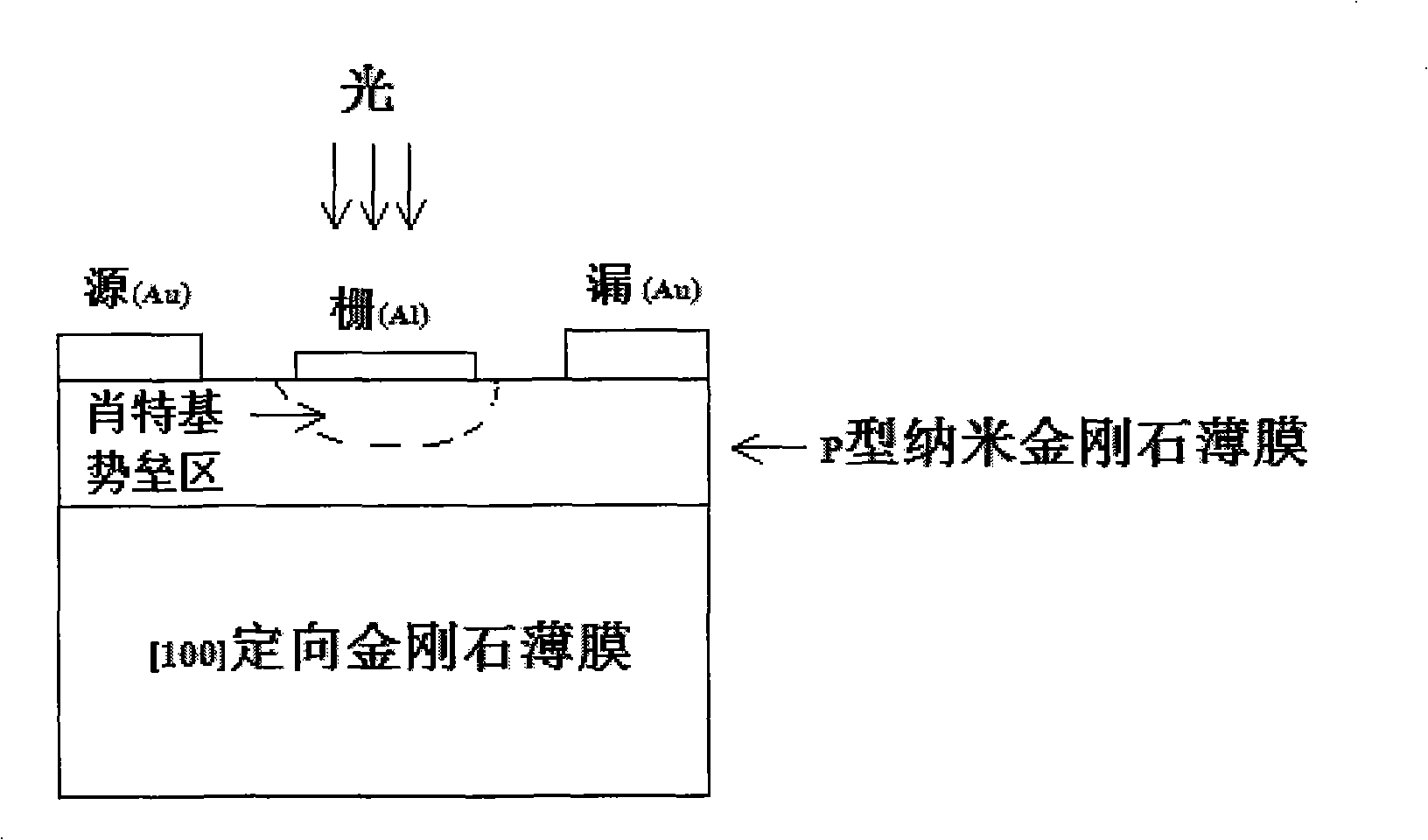
Preparing method of diamond thin-film field-effect photo-electric detector
A technology of diamond thin film and photodetector, which is applied to circuits, electrical components, semiconductor devices, etc., to achieve the effect of reducing manufacturing cost, promoting large-scale application, and improving smoothness
- Summary
- Abstract
- Description
- Claims
- Application Information
AI Technical Summary
Problems solved by technology
Method used
Image

Examples
Embodiment
[0030] Embodiment: the technical process and steps of the present embodiment are as follows:
[0031] (1) Silicon substrate pretreatment: (100) mirror-polished silicon wafers were used as deposition substrates. Ultrasonic cleaning with HF acid for 10 minutes to remove the silicon oxide layer on the surface. In order to increase the nucleation density of the diamond film, the silicon substrate was mechanically ground for 10 minutes using diamond powder with a particle size of 100 nm. The ground silicon wafer was ultrasonically cleaned in an acetone solution mixed with 100 nm diamond powder for 10 minutes. Finally, the silicon wafer is ultrasonically cleaned with deionized water and acetone, respectively, until the surface of the silicon wafer is clean, dried and put into the reaction chamber of a microwave plasma chemical vapor deposition (MPCVD) device.
[0032] (2) Diamond film nucleation process: first use a vacuum pump to evacuate the reaction chamber to 5Pa, and then use...
PUM
| Property | Measurement | Unit |
|---|---|---|
| Thickness | aaaaa | aaaaa |
Abstract
Description
Claims
Application Information