

Method for preparing bismuth nano wire array thermoelectric materials
A technology of line array and thermoelectric materials, which is applied in the field of thermoelectric materials and semiconductor materials preparation, can solve the problems of low filling rate of nanowires, inaccurate control of deposition time, inability to control large area and single size, etc., and achieve wide commercial application Foreground, launch stability, low cost effect
- Summary
- Abstract
- Description
- Claims
- Application Information
AI Technical Summary
Problems solved by technology
Method used
Image

Examples
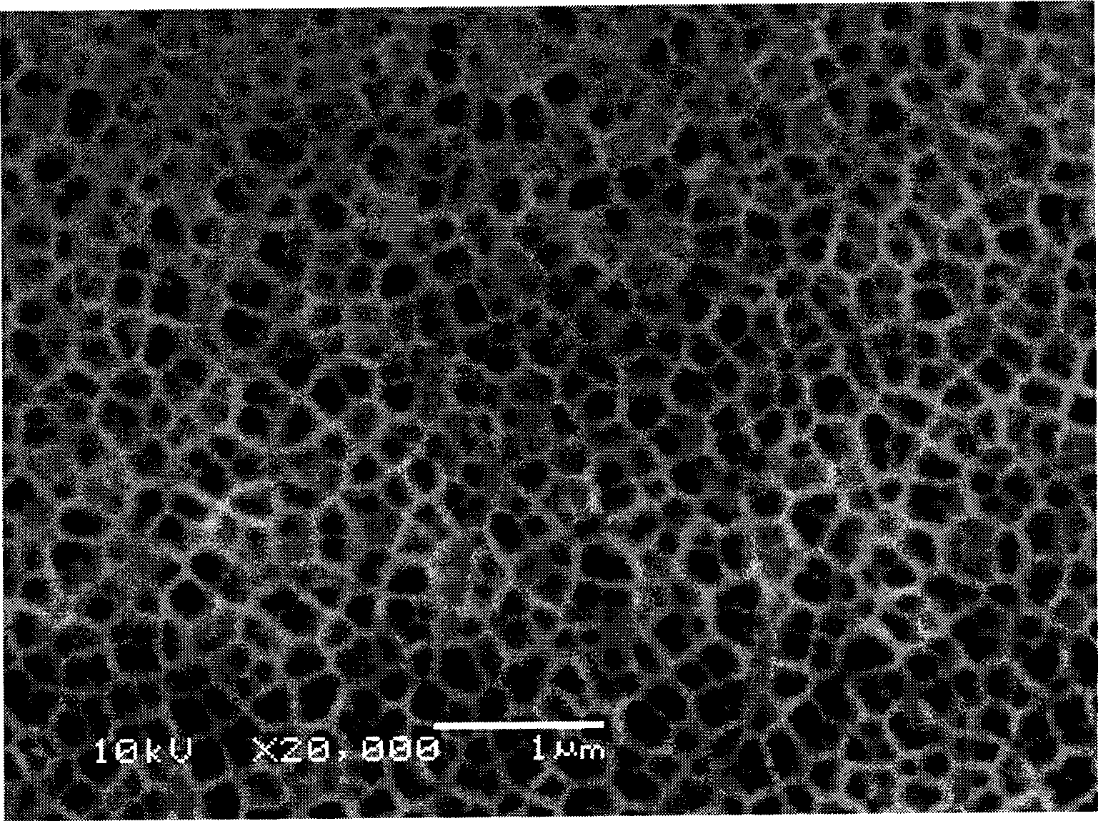
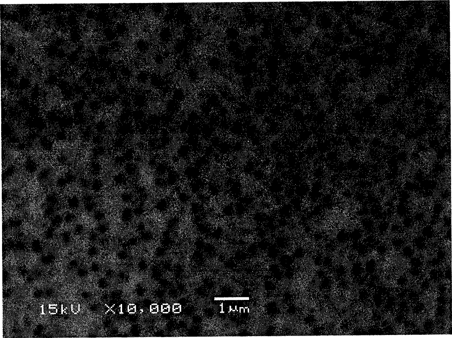
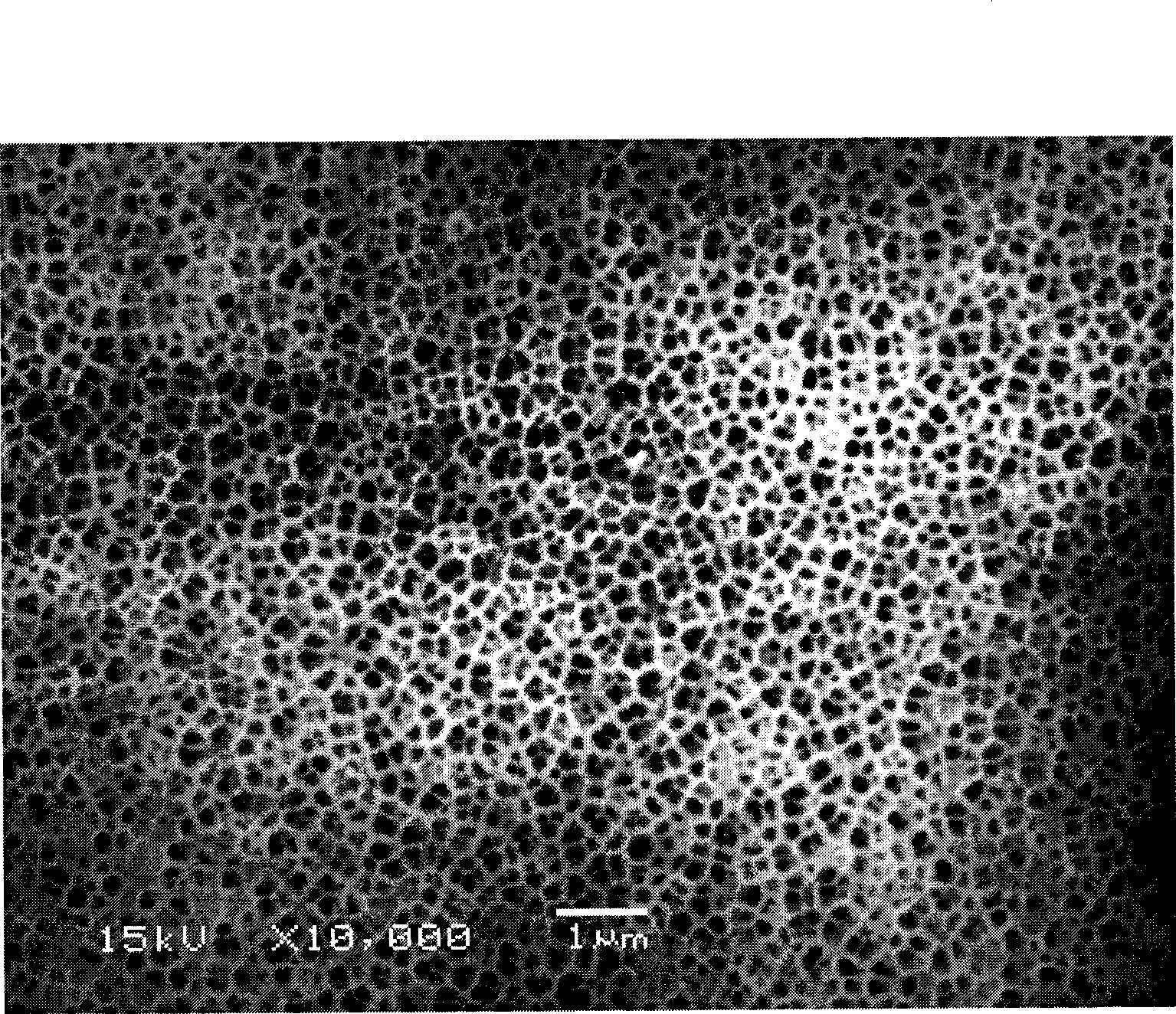
Embodiment 1
[0018] a) Cut the alumina template into small pieces of 1cm×2cm, and then ultrasonically clean them in alcohol solution.
[0019] b), prepare electrodeposition solution, this solution is made of 10g / l BiCl 3 , 50g / l tartaric acid, 95g / l glycerol and 50g / l NaCl solution, the pH of the solution was adjusted to 0.9 with dilute hydrochloric acid.
[0020] c) Use CHl660C electrochemical workstation to conduct electrodeposition on alumina template, and select cyclic voltammetry, step 1: -1v step time 20ms; step 2: 0V step time 10ms; step 3: 1V The step time is 30ms as a cycle; the step cycle is cycled, the deposition time is controlled for 120 minutes, the electrochemical deposition software is closed, and the deposition is ended.
[0021] d) After the electrodeposition is completed, the template is taken out, placed in deionized water, ultrasonically cleaned, then placed in a NaOH (0.5mol / l) solution, and left to stand for 30 minutes to remove the aluminum oxide film.
[0022] e)...
PUM
 Abstract
Description
Claims
Application Information