

Double-beam holographic interference multiple exposure method for preparing two-dimensional photonic crystal
A two-dimensional photonic crystal and holographic interference technology, applied in the field of semiconductor optoelectronic devices, can solve problems such as affecting the periodicity and uniformity of photonic crystal lattices, complicating experimental equipment, affecting interference patterns, etc., achieving low price and simple and convenient operation. , high precision effect
- Summary
- Abstract
- Description
- Claims
- Application Information
AI Technical Summary
Problems solved by technology
Method used
Image

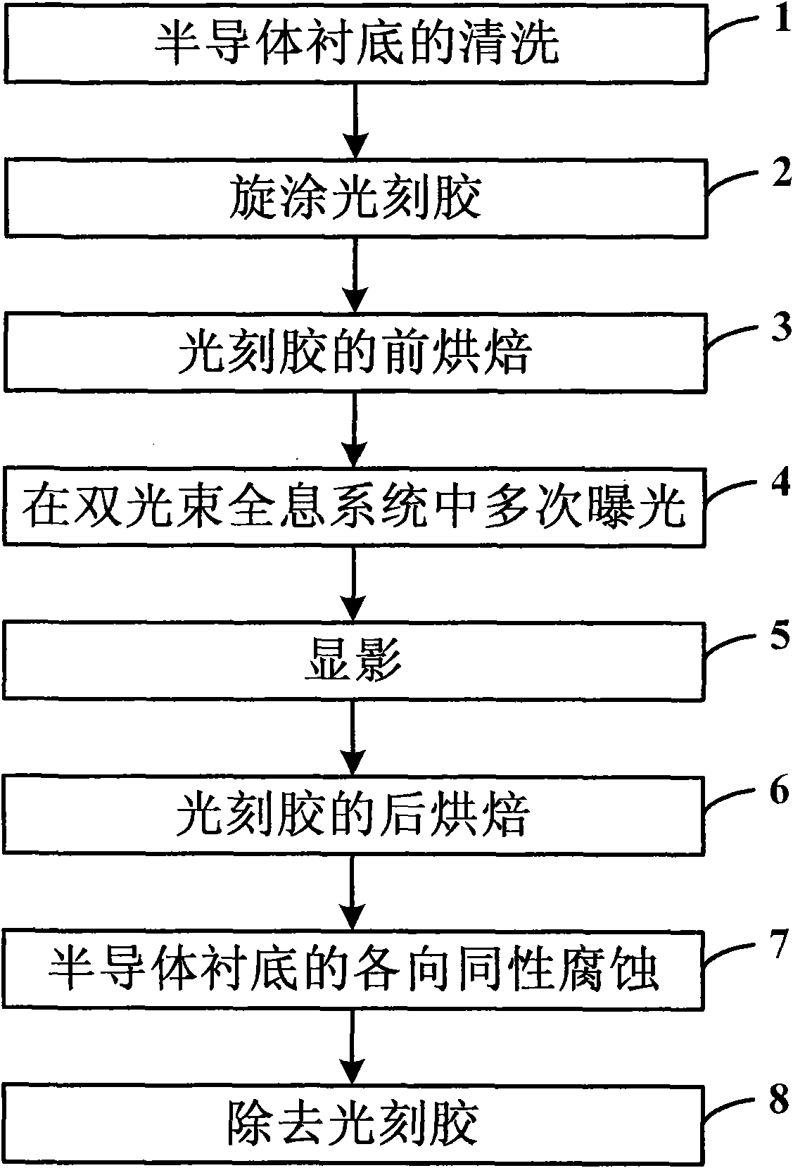
Examples
example 1
[0087] Example 1: Preparation of two-dimensional photonic crystals with square lattice circular hole elements
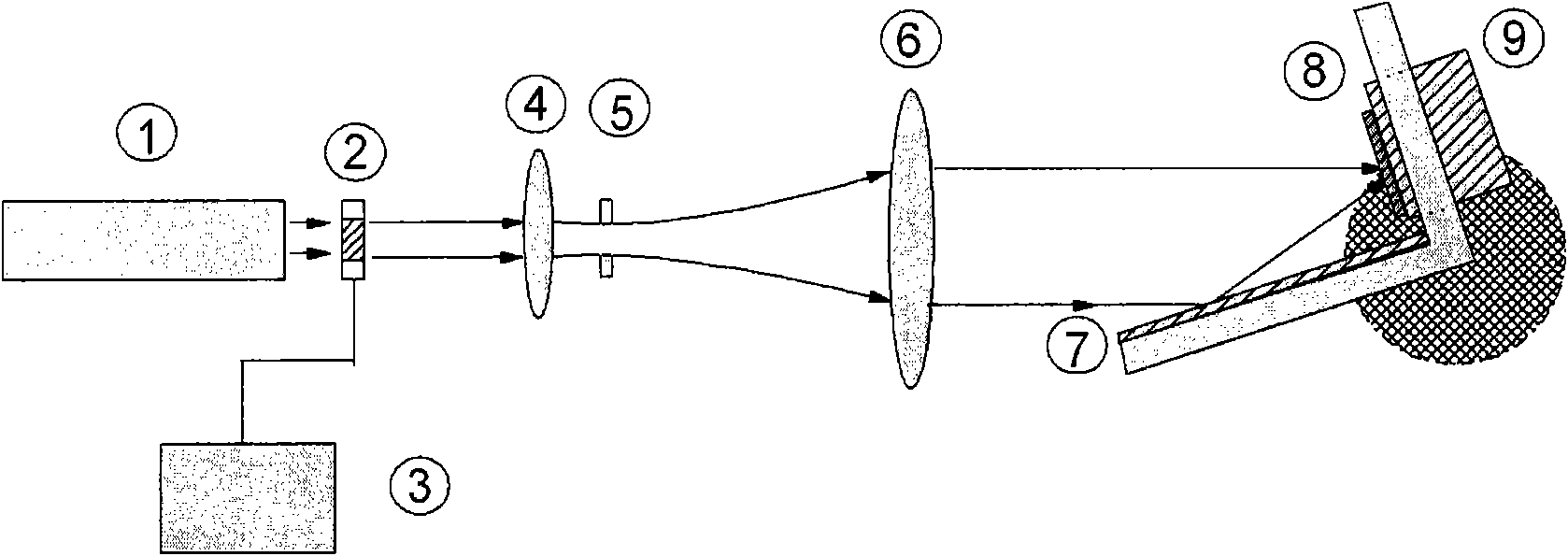
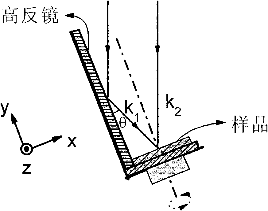
[0088] It can be known from formula (2) that adjusting the angle between two beams of coherent light can change the period of interference fringes. To this end, turn the motorized turntable so that the angle θ between the light beam and the high-reflection flat mirror fixed on the turntable is 10.6°, and the interference fringe period is 1.2 μm. The photoresist sample that has been properly pre-baked is fixed on the other end of the rotating bracket and exposed for 90 seconds. Exposure time is controlled by an electronic timer and shutter. After the exposure, the sample was rotated 90° for the second exposure, and the exposure time was 100 seconds. Next, put the sample into a developing solution prepared by tetramethylammonium hydroxide and water at a volume ratio of 1:10 for development, then harden the film, corrode, remove the glue, rinse with deionized water, a...
example 2
[0090] Example 2: Preparation of two-dimensional photonic crystals with rectangular lattice and elliptical hole primitives
[0091] On the InP substrate, the photoresist will be spin-coated and placed in such as image 3 In the interference field shown, θ is 10.6°. After exposure for 90 seconds, turn the high-reflectivity plane mirror to the position where θ is 5.28°, and rotate the sample by 90° for the second exposure, and the exposure time is also 90 seconds. Next, put the sample into a developing solution prepared by tetramethylammonium hydroxide and water at a volume ratio of 1:10 for development, then harden the film, corrode, remove the glue, rinse with deionized water, and blow dry with nitrogen. Among them, the development time and etching time need to be precisely controlled to control the duty cycle and depth of the circular hole.
[0092] Figure 11 It is the pattern of the photoresist under a 1500 times optical microscope, the lattice constants are 1.2 μm and 2...
example 3
[0093] Example 3: Preparation of two-dimensional photonic crystals with circular holes in a hexagonal lattice
[0094] On the InP substrate, the photoresist will be spin-coated and placed in such as image 3 In the interference field shown, θ is 10.6°. After 60 seconds of exposure, keep the rotation angle θ of the electric rotary table unchanged, and at the same time rotate the sample by ±60° for the second and third exposures, and the exposure time remains unchanged. Then put the sample into a developing solution prepared by tetramethylammonium hydroxide and water at a volume ratio of 1:10 for development, then harden the film, corrode, remove the glue, rinse with deionized water, and blow dry with nitrogen. Among them, the development time and etching time need to be precisely controlled to control the duty cycle and depth of the circular hole.
[0095] Figure 13 It is a pattern of photoresist under a 1500 times optical microscope, the lattice constants are 1.2 μm, the t...
PUM
| Property | Measurement | Unit |
|---|---|---|
| depth | aaaaa | aaaaa |
| thickness | aaaaa | aaaaa |
Abstract
Description
Claims
Application Information