

Method for manufacturing selective emitter junction of multricrytalline silicon solar cell
A solar cell and selective technology, applied in circuits, electrical components, semiconductor devices, etc., can solve the problems of difficult matching of sintering temperature, diffusion temperature, serious phosphorus volatilization, and long process time, so as to achieve improved open circuit voltage Voc and high photoelectric conversion Efficiency, the effect of improving the collection rate
- Summary
- Abstract
- Description
- Claims
- Application Information
AI Technical Summary
Problems solved by technology
Method used
Image

Examples
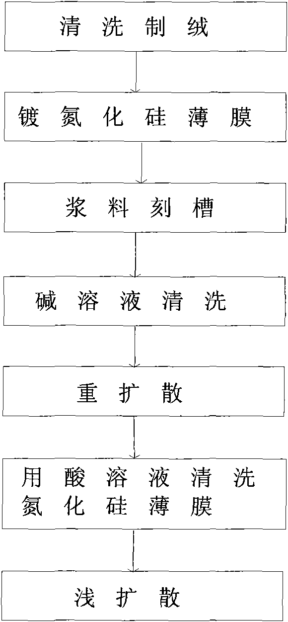
Embodiment 1
[0027] In order to remove the mechanical damage layer on the surface of the silicon wafer and remove the surface oil and metal impurities to form an uneven suede surface and increase the absorption of sunlight by the silicon wafer, the silicon wafer is first cleaned and textured, and then PECVD technology is used on the surface of the silicon wafer Coating a layer of silicon nitride film, the coating temperature is 200 ℃ ~ 500 ℃, the film thickness is 5nm ~ 200nm, and then use screen printing technology to print the corrosive paste on the surface of silicon nitride for slotting to obtain the required Silicon nitride mask, the shape of the groove is the shape of the electrode, the corrosive slurry is 1% to 50% of ammonium hydrogen fluoride and organic matter, the drying temperature is 200°C to 500°C, and the time is 5 to 30min. After drying Wash the reactants with an alkaline solution, and then perform re-diffusion at a diffusion temperature of 890°C to 950°C. After heavy doping...
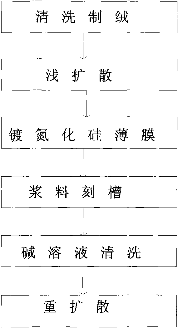
Embodiment 2
[0029] After the silicon wafer is cleaned and textured, shallow diffusion is carried out. The diffusion process is the same as the conventional process, and then PECVD technology is used to coat a layer of silicon nitride film on the surface of the silicon wafer. The coating temperature is 200 ° C ~ 500 ° C, and the film thickness is 5 nm ~ 200 nm. , and then use screen printing technology to print the corrosive slurry on the surface of silicon nitride for slotting to obtain the required silicon nitride mask. The shape of the groove is the shape of the electrode, and the corrosive slurry is 1% to 50 % ammonium hydrogen fluoride and organic matter, the drying temperature is 200 ° C ~ 500 ° C, the time is 5 ~ 30 minutes, after drying, the reactants are cleaned with alkaline solution, and then re- Diffusion, forming a selective emission junction.
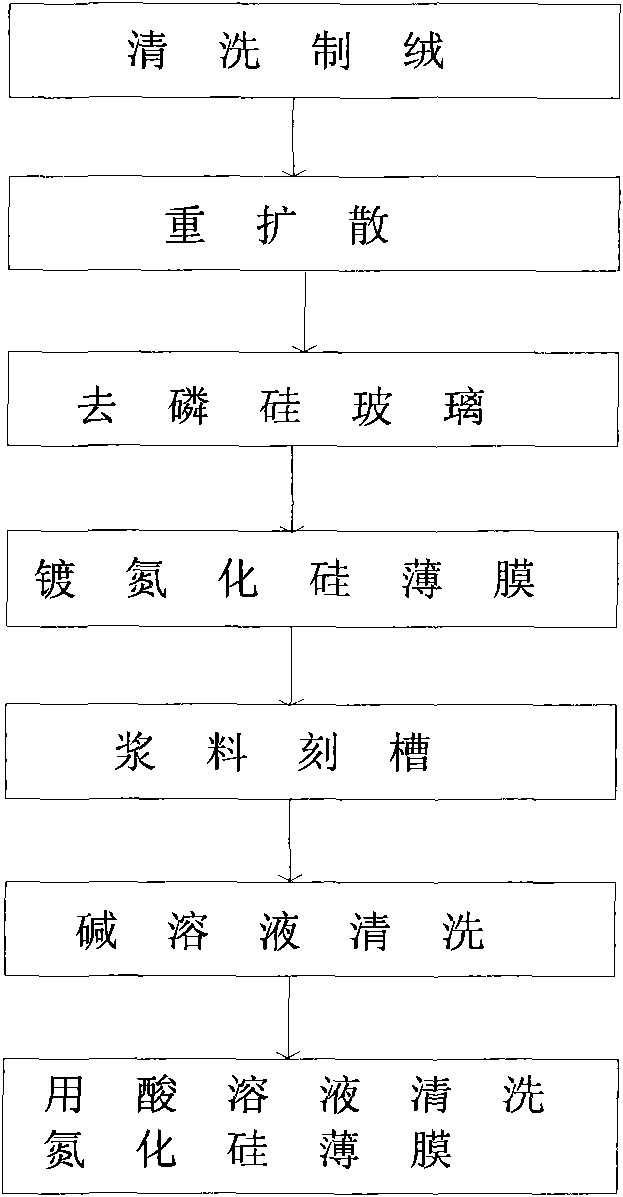
Embodiment 3
[0031] After the silicon wafer is cleaned and textured, re-diffusion is carried out. The diffusion temperature is 890°C-950°C. After removing the phosphosilicate glass, PECVD technology is used to coat a layer of silicon nitride film on the surface of the silicon wafer. The coating temperature is 200°C-500°C. The thickness is 5nm to 200nm, and then the corrosive paste is printed on the surface of silicon nitride by screen printing technology to make grooves to obtain the required silicon nitride mask. The grooved area is the non-electrode area, and the corrosive paste The material is 1% to 50% ammonium hydrogen fluoride and organic matter. The drying temperature is 200°C to 500°C and the time is 5 to 30min. After drying, the reactants are cleaned with an alkaline solution. The cleaning time and solution The concentration is related, after cleaning for a certain period of time, a shallowly doped region can be obtained, and then use 1% to 30% hydrofluoric acid solution or 1% to 5...
PUM
| Property | Measurement | Unit |
|---|---|---|
| Thickness | aaaaa | aaaaa |
| Thickness | aaaaa | aaaaa |
Abstract
Description
Claims
Application Information