Resistive random access memory based on bismuth iron thin film system and manufacturing method thereof

A resistive random, bismuth ferrite technology, applied in static memory, digital memory information, information storage, etc., can solve the problems of slow speed, high operating voltage, poor endurance, etc., and achieve good electro-resistance effect and stable resistance value , good stability effect

Active Publication Date: 2009-11-25
NINGBO INST OF MATERIALS TECH & ENG CHINESE ACADEMY OF SCI
View PDF0 Cites 40 Cited by
  • Summary
  • Abstract
  • Description
  • Claims
  • Application Information

AI Technical Summary

Problems solved by technology

At present, the mainstream non-volatile memory is flash memory (Flash Memory), but flash memory has problems such as high operating voltage, slow speed, and poor endu...

Method used


Image

  • Resistive random access memory based on bismuth iron thin film system and manufacturing method thereof
  • Resistive random access memory based on bismuth iron thin film system and manufacturing method thereof
  • Resistive random access memory based on bismuth iron thin film system and manufacturing method thereof

Examples


Embodiment 1

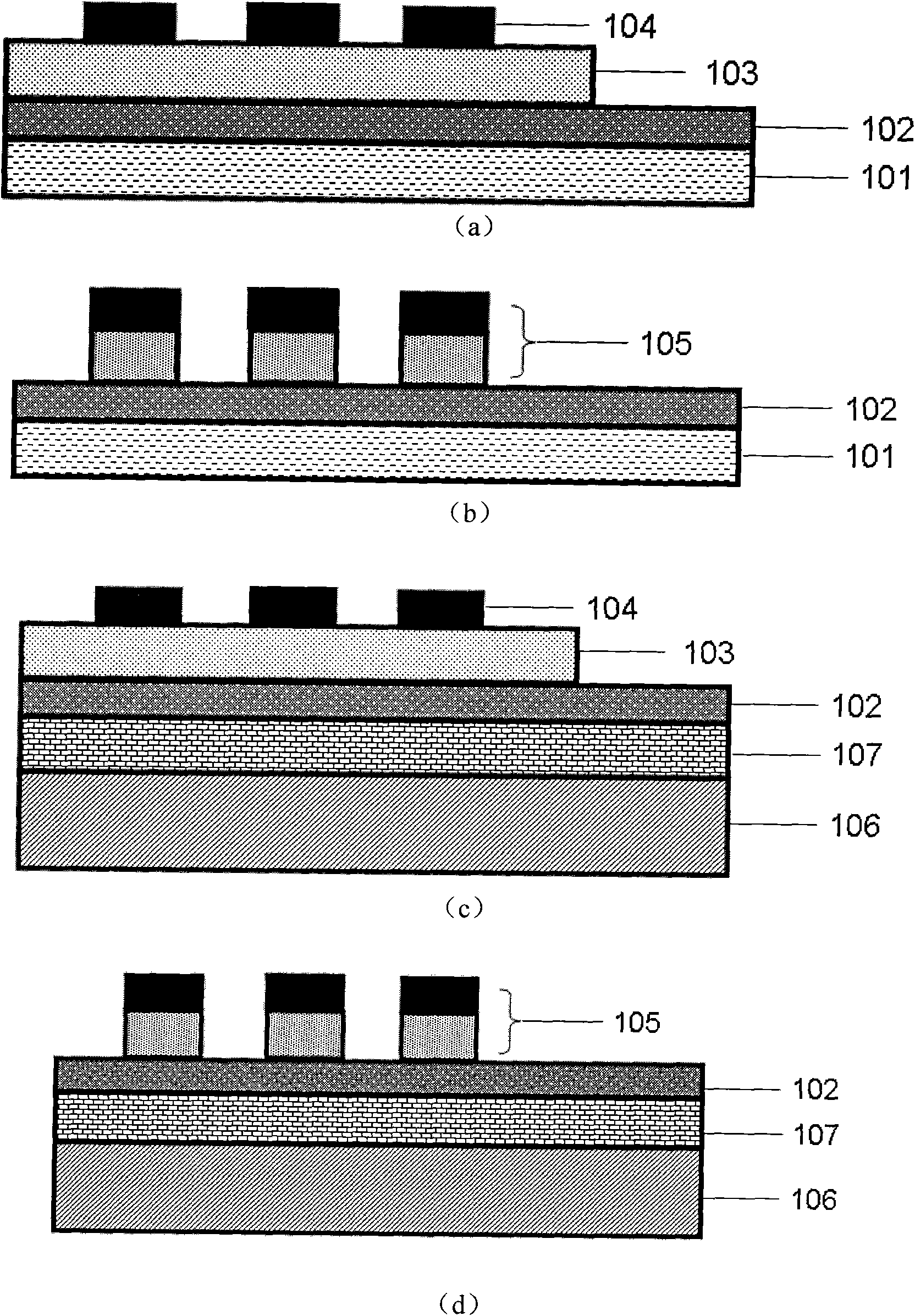
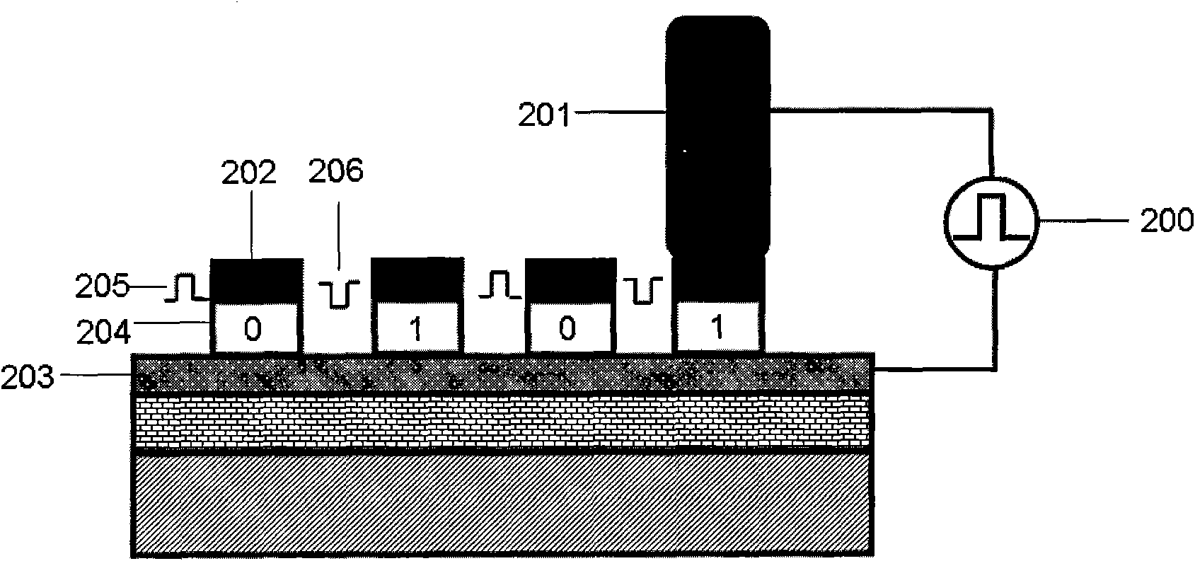
[0039] like figure 1 In (c), the silicon dioxide dielectric isolation layer 107 with a thickness of about 400nm is oxidized on the single crystal silicon base layer 106 by thermal oxidation, and the silicon dioxide dielectric isolation layer 107 is oxidized by thermal evaporation or magnetron sputtering 2 Growth Pt / Ti (the thickness of Pt is respectively 100nm, the thickness of Ti is 50nm, used as bonding layer) lower electrode 102 on dielectric isolation layer 107; Then grow bismuth ferrite thin film on lower electrode 102; Finally by electron beam evaporation, A 200 nm thick Cu upper electrode 104 is prepared by using a mask (the mask is uniformly distributed 100 μm circular holes), and the size of the electrode is 100 μm.

[0040] Among them, the bismuth ferrite thin film is prepared by the sol-gel method, and the specific process is as follows:

[0041] (1) Weigh iron nitrate (Fe(NO 3 ) 3 9H 2 O) and bismuth nitrate (Bi(NO 3 ) 3 ·5H 2 O), dissolved in ethylene glyc...

Embodiment 2

[0047] The main difference between embodiment 2 and embodiment 1 is: the recording medium used in embodiment 2 is lanthanum (La) doped BiFeO 3 Thin films in which the molar ratio of lanthanum is 5%, i.e. La 0.05 Bi 0.95 FeO 3 , the annealing temperature is 550°C.

[0048] Oxidize about 400nm thick silicon dioxide dielectric isolation layer 107 on the monocrystalline silicon base layer 106 by thermal oxidation, and grow Pt / Ti (Pt) on the silicon dioxide dielectric isolation layer 107 by thermal evaporation or magnetron sputtering Thickness is 100nm, the thickness of Ti is 50nm, as bonding layer) lower electrode 102, then grow the bismuth ferrite thin film doped with lanthanum on the lower electrode 102, finally by electron beam evaporation, adopt the method of mask plate to prepare 200nm thick The Cu upper electrode 104 has a size of 100 μm.

[0049] Wherein, the above-mentioned bismuth ferrite film is prepared by a sol-gel method, and the specific process is as follows:

...

Embodiment 3

[0054] The main difference between embodiment 3 and embodiment 2 is: the upper electrode of embodiment 3 adopts Ag electrode.

[0055] Oxidize SiO with a thickness of about 400 nm on the single crystal silicon base layer 106 by thermal oxidation 2 The dielectric isolation layer 107 is formed on SiO by thermal evaporation or magnetron sputtering 2 A lower electrode 102 of Pt / Ti (with a thickness of 100 nm / 50 nm) is grown on the dielectric isolation layer 107 .

[0056] The above-mentioned bismuth ferrite thin film is prepared by a sol-gel method.

[0057] The specific process is:

[0058] (1) Weigh iron nitrate (Fe(NO 3 ) 3 9H 2 O), bismuth nitrate (Bi(NO 3 ) 3 ·5H 2 O) and La(NO 3 ) 3 ·6H 2 O dissolved in ethylene glycol methyl ether (C 3 h 8 o 2 ) and ethylene glycol (C 2 h 6 o 2 ) in the mixed solution, and add an appropriate amount of acetic acid (C 2 h 4 o 2 ), adjust the pH value at about 2-3, so that the concentration of the bismuth ferrite sol obtain...


PUM

PropertyMeasurementUnit
Thicknessaaaaaaaaaa
Thicknessaaaaaaaaaa
Sizeaaaaaaaaaa

Abstract

The invention relates to a resistive random access memory based on bismuth iron thin film system and manufacturing method thereof. The memory comprises an insulating substrate (101) layer as the first layer, a lower electrode (102) as the second layer, a bismuth iron thin film (103) as the third layer, an upper electrode (104) as the fourth layer; the manufacturing method utilizes the method thermal evaporation or magnetron sputtering to grow the lower electrode on the insulating substrate layer, utilizes the method of magnetron sputtering, pulsed laser deposition or colloidal sol-gel to grow the bismuth iron thin film on the lower electrode, finally utilizes the method of thermal evaporation or magnetron sputtering to grow the upper electrode on the bismuth iron thin film, and utilizes the method of ultraviolet lithography, electron beam or ion beam etching to obtain the electrode pattern. The memory provided by the invention has excellent electroluminescent resistance effect and good stability, and has simple manufacturing method, low cost and is easy for manufacturing in large scale and commercial process.

Description

technical field [0001] The invention relates to the technical field of non-volatile memory, in particular to a resistive RAM based on BiFeO3 base film and a preparation method thereof. Background technique [0002] The high-speed development of information technology depends on large-capacity, high-speed, non-volatile information storage technology. Non-volatile information storage technology has the advantage of maintaining information data when the power is cut off, and has been widely used in computer, automobile, modern industry and other fields. At present, the mainstream non-volatile memory is flash memory (Flash Memory), but flash memory has problems such as high operating voltage, slow speed, and poor endurance. With the continuous improvement of information storage technology requirements, it is necessary to develop low-power, High-speed, long-retention non-volatile memory. Currently, ferroelectric random access memory (FeRAM), magnetic random access memory (MRAM)...

Claims


Application Information

Patent Timeline
IPC IPC(8): H01L45/00G11C11/56C23C20/08
Inventor 李润伟尹奎波刘宜伟李蜜陈斌
Owner NINGBO INST OF MATERIALS TECH & ENG CHINESE ACADEMY OF SCI
Why Eureka
Try Eureka