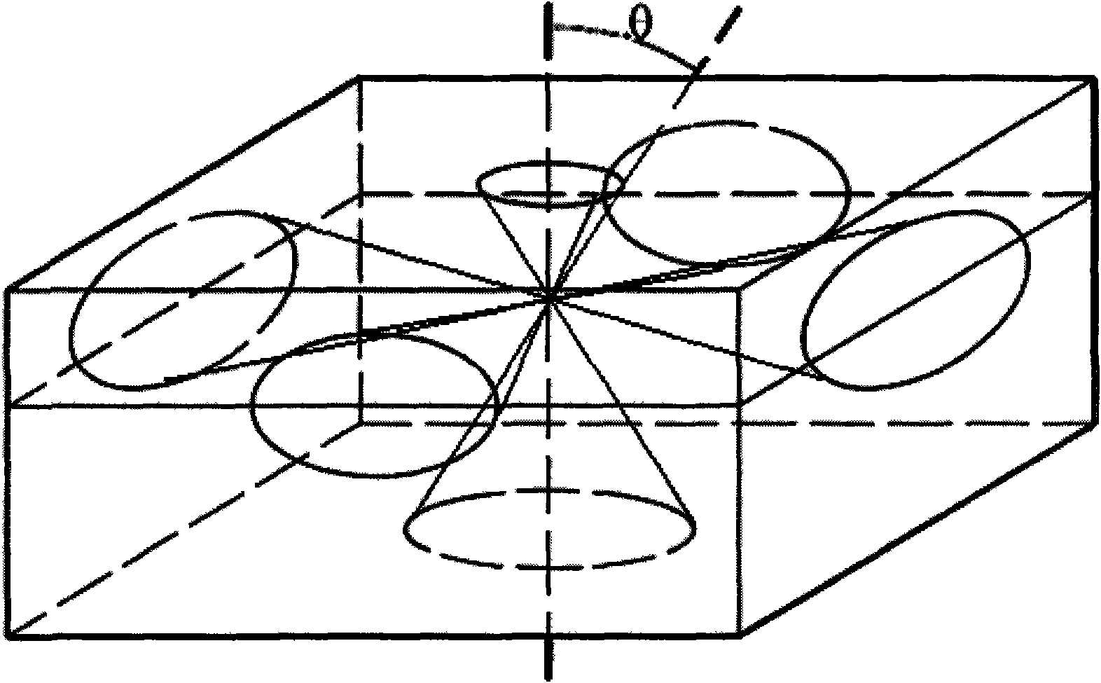
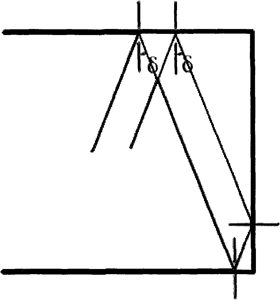
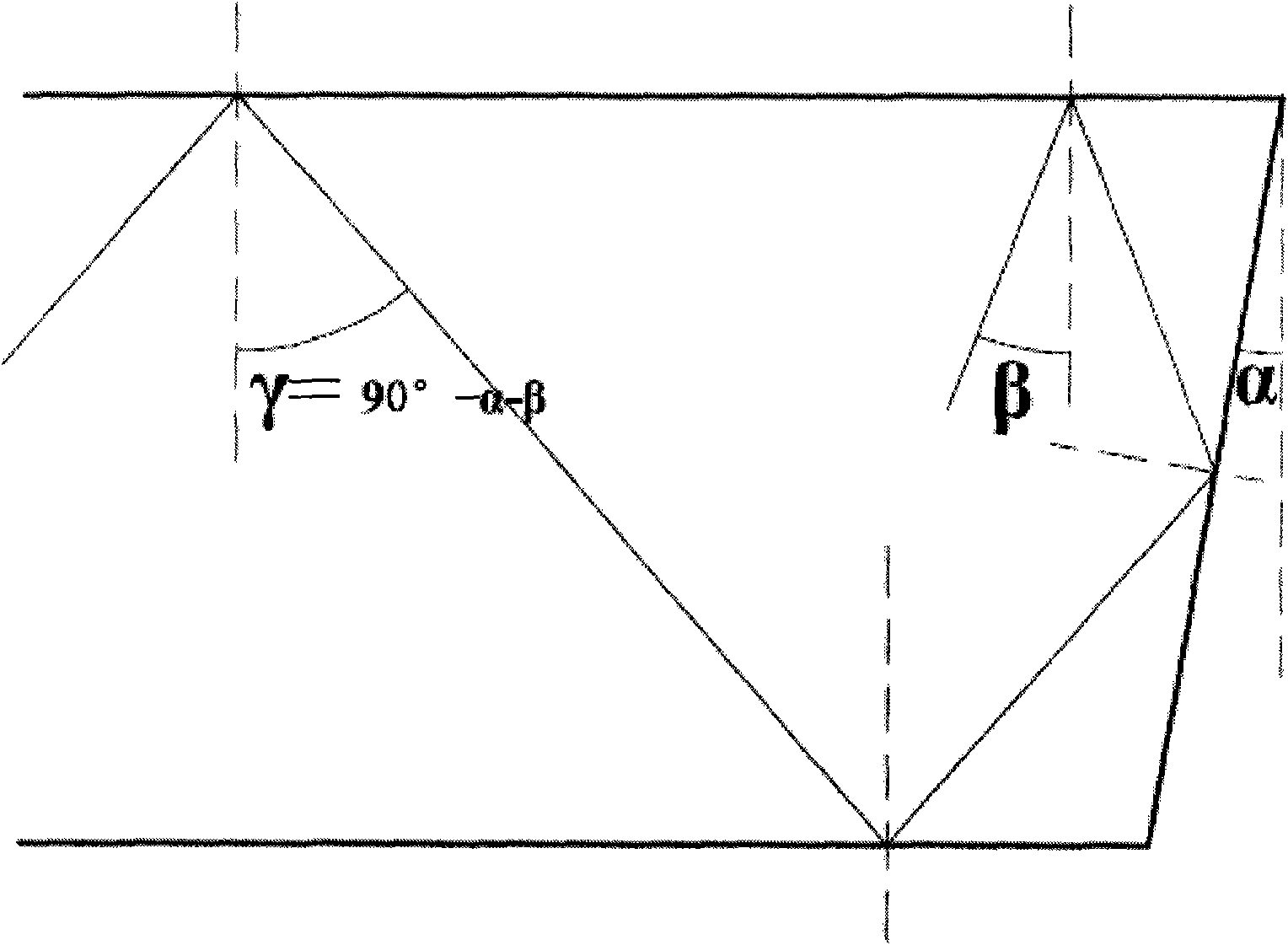
Laterally inclined LED chip and preparation method thereof
A technology of light-emitting diodes and chips, which is applied in the direction of electrical components, circuits, semiconductor devices, etc., can solve the problems of low light-emitting efficiency of light-emitting diode chips, and achieve the effects of improving light-emitting efficiency, reducing stress, and improving thinning
- Summary
- Abstract
- Description
- Claims
- Application Information
AI Technical Summary
Problems solved by technology
Method used
Image
Examples
Embodiment
[0037] Embodiment: Take a gallium nitride-based light-emitting diode with sapphire as the substrate 1 as an example.
[0038]A buffer layer 2, a gallium nitride N-type layer 3, a multiple quantum well layer 4 and a gallium nitride P-type layer 5 are epitaxially grown on the sapphire substrate 1. Isolation photolithography and dry etching are performed to form an N-type gallium nitride mesa; a nickel / gold transparent conductive layer 6 is evaporated (the thickness of the nickel layer is 10-50 The thickness of the gold layer is 30~100 ); Making N electrode 8; Making P electrode 9; Evaporating silicon dioxide passivation layer 7. See the following steps Figure 6 , The pattern window is lithographically and etched on the silicon dioxide passivation layer 7; fused phosphoric acid and ICP dry etching are used together to etch the epitaxial part at the position of the pattern window, through the temperature, light, time, and etching gas group Conditions such as separation and etchin...
PUM
 Abstract
Description
Claims
Application Information


