
Resistive random access memory and manufacturing method thereof

A resistive memory, parylene technology, applied in the field of flexible electronics, can solve the problems of inability to defend against solvents, limit storage density, inability to miniaturize and high-density applications, and achieve good process compatibility and improve storage density. Effect

Inactive Publication Date: 2010-01-20
SEMICONDUCTOR MANUFACTURING INTERNATIONAL (BEIJING) CORP +1
View PDF0 Cites 27 Cited by
  • Summary
  • Abstract
  • Description
  • Claims
  • Application Information

AI Technical Summary

Problems solved by technology

However, most of the organic RRAM materials reported so far cannot resist the solvents used in the photolithography process, so they cannot be miniaturized and high-density applications
The preparation of organic resistive memory reported in the literature generally adopts spin-coating and hard mask technology, and the device unit size is generally relatively large (on the order of square millimeters), which limits its storage density.
Moreover, the spin coating process is prone to residual pollution after solvent volatilization and compatibility with other modules

Method used


Image

  • Resistive random access memory and manufacturing method thereof
  • Resistive random access memory and manufacturing method thereof
  • Resistive random access memory and manufacturing method thereof

Examples


Embodiment Construction

[0027] Below in conjunction with accompanying drawing and specific embodiment the present invention is described in further detail:

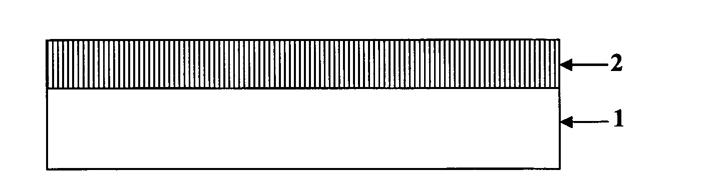
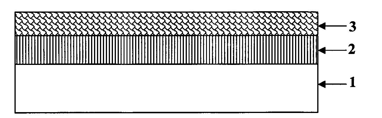
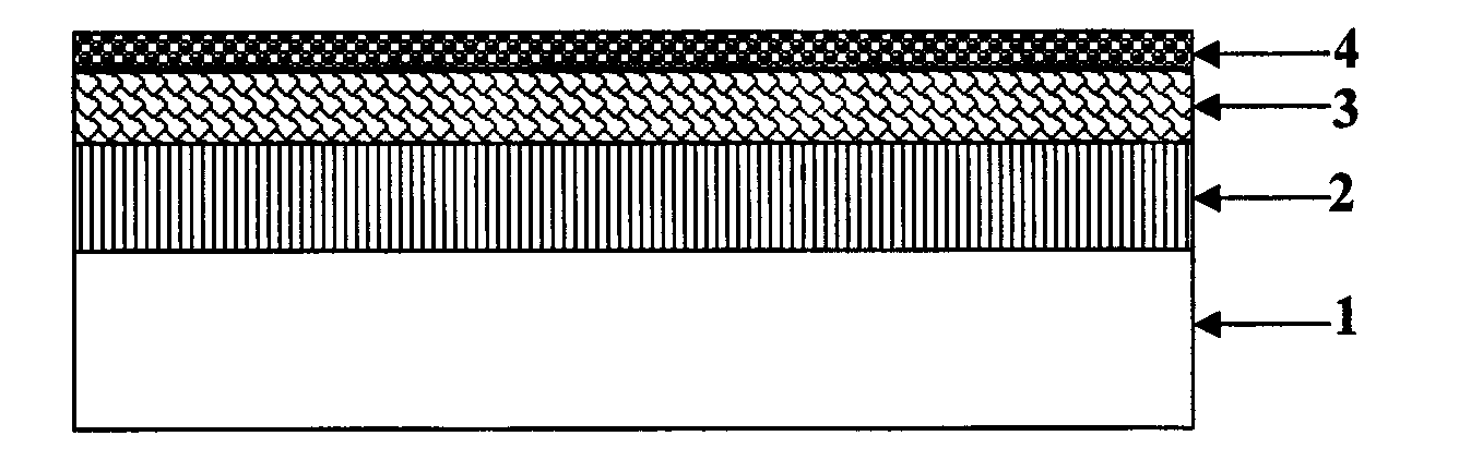
[0028] Referring to Figure 1, the preparation of the resistive memory of the present invention is specifically as follows:

[0029] 1) On the silicon substrate 1, tungsten metal in a conventional CMOS process is used as the lower electrode 2; the lower electrode adopts a physical vapor deposition (PVD) method, and the tungsten electrode can be patterned by standard photolithography and wet etching techniques, Figure 1(a);

[0030] 2) Use polymer chemical vapor deposition (Polymer CVD) technology to deposit parylene-C type (Parylene-C film 3, with a thickness of 50-150nm, as shown in Figure 1(b); CVD equipment, process selection equipment standard parameters, deposition rate between 1nm / min and 10nm / min;

[0031] 3) Utilize the physical vapor deposition method to deposit the gold nanolayer 4 of 6-20nm, as shown in Figure 1 (c);

[0032] 4) By ...


PUM

PropertyMeasurementUnit
Thicknessaaaaaaaaaa
Thicknessaaaaaaaaaa
Thicknessaaaaaaaaaa

Abstract

The invention discloses a resistive random access memory (RAM) and a manufacturing method thereof, belonging to the technical field of integrated circuits. The resistive RAM is of MIM structure, wherein, the bottom layer and the top layer of the MIM structure are respectively provided with metal electrodes; the intermediate layer of the MIM structure is provided with a first layer parylene polymer membrane, a metal or metal oxide nano-layer and a second layer parylene polymer membrane. By adopting the composition of a parylene polymer and metal / metal oxide as a resistive material, the invention can manufacture the resistive RAM with good resistive property and process compatibility. A preparation method of the parylene polymer adopts the chemical vapor deposition process at room temperature without by-products and solvent pollution, and is compatible with other modules of CMOS. Besides, the solution and solvents used in the parylene-resistant standard photolithography process can employ the CMOS standard photolithography process to manufacture the resistive RAM, thus increasing the memory density of the RAM.

Description

technical field [0001] The invention relates to a nonvolatile (Nonvolatile memory) resistive random access memory (RRAM: Resistive Random Access Memory) and a manufacturing method, belonging to the technical fields of flexible electronics, polymer and CMOS hybrid integrated circuits. Background technique [0002] The 21st century is a high-tech era of information digitization. The explosive growth of information and the continuous miniaturization of electronic devices have put forward higher requirements for storage technology, and there is an urgent need for breakthroughs in storage materials and technologies. Research and development of memory with higher storage density, lower power consumption, faster response speed and repeatable reading and writing has become a hot spot in the electronic field. At present, the most widely used and most developed non-volatile memory is flash memory (flash memory), but its disadvantages such as slow writing speed and high power consumpti...

Claims


Application Information

Patent Timeline
IPC IPC(8): H01L51/05H01L51/40
Inventor 邝永变黄如唐昱张丽杰
Owner SEMICONDUCTOR MANUFACTURING INTERNATIONAL (BEIJING) CORP
Features
  • Generate Ideas
  • Intellectual Property
  • Life Sciences
  • Materials
  • Tech Scout
  • Unparalleled Data Quality
  • Higher Quality Content
  • 60% Fewer Hallucinations
Learn More