Preparation method of thin film of diffusion impervious layer

A technology of barrier layer and thin film, which is applied in the direction of coating, metal material coating process, semiconductor/solid-state device manufacturing, etc., can solve the problem of inability to effectively block copper diffusion, and achieve the effect of improving performance and increasing working temperature

Inactive Publication Date: 2010-03-17
HARBIN INST OF TECH
View PDF0 Cites 14 Cited by
  • Summary
  • Abstract
  • Description
  • Claims
  • Application Information

AI Technical Summary

Problems solved by technology

[0003] The purpose of the present invention is to solve the problem that the existing Ru-N film diffusion barrier layer between copper and silicon cannot effectively block copper (Cu) atoms and silicon (Si) atoms Diffusion problem between; And provide the preparation method of Ru-TiN diffusion barrier film

Method used


Image

  • Preparation method of thin film of diffusion impervious layer
  • Preparation method of thin film of diffusion impervious layer
  • Preparation method of thin film of diffusion impervious layer

Examples


specific Embodiment approach 1

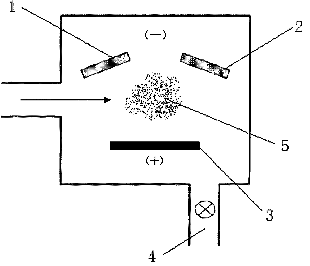
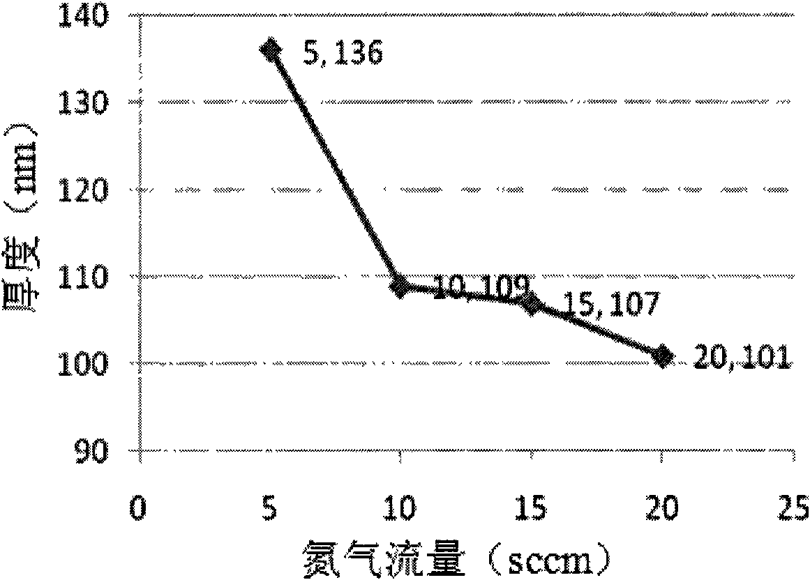
[0007] Specific embodiment one: the preparation method of the diffusion barrier film in the present embodiment is realized by following steps: one, silicon substrate is put into the vacuum chamber of magnetron sputtering coating equipment, utilize plasma to silicon substrate Sputtering cleaning; 2. Under the atmosphere of nitrogen and argon, use ruthenium and titanium as the target cathode and adopt the magnetron co-sputtering method to carry out the deposition process on the silicon substrate processed by step 1 for 600s (obtain the deposited state on the silicon substrate. thin film), wherein during the deposition process, the sputtering power of target cathode ruthenium is 100W, the sputtering power of target cathode titanium is 100-220W, the flow rate of argon gas is 10-25 sccm, the flow rate of nitrogen gas is 5-20 sccm, and the working pressure Fixed at 10mTorr; 3. Heat up to 400-700°C at a heating rate of 10°C / min, heat the silicon substrate treated in step 2 for 60 minu...

specific Embodiment approach 2

[0023] Embodiment 2: This embodiment differs from Embodiment 1 in that the silicon substrate described in step 1 is a single crystal silicon polished wafer. Other steps and parameters are the same as those in Embodiment 1.

specific Embodiment approach 3

[0024] Embodiment 3: The difference between this embodiment and Embodiment 1 or 2 is that the sputtering power of the target cathode titanium (Ti) in step 2 is 130-190W. Other steps and parameters are the same as those in Embodiment 1 or Embodiment 2.


PUM

PropertyMeasurementUnit
thicknessaaaaaaaaaa
electrical resistivityaaaaaaaaaa

Abstract

A preparation method of a thin film of a diffusion impervious layer relates to a preparation method of a new diffusion impervious layer between copper and silicon in an integrated circuit. The preparation method solves the problem that an N element in the existing diffusion impervious layer Ru-N between copper and silicon easily overflows at high temperature, thus causing the Ru-N diffusion impervious layer to lose efficacy. The preparation method comprises the following steps: 1. cleaning a silicon substrate; 2. using a magnetic control sputtering method for depositing the thin film; and 3. obtaining the Ru-N diffusion impervious layer after annealing. The method has simple technology; and the obtained Ru-N diffusion impervious layer can effectively inhibit the diffusion between copper atoms and silicon atoms.

Description

technical field [0001] The invention relates to a preparation method of a diffusion barrier layer between copper and silicon in a concentrated circuit. Background technique [0002] With the continuous improvement of chip integration, the line width and size of interconnection materials continue to shrink, and the performance of Al as an interconnection material has been difficult to meet the requirements of integrated circuits. Compared with Al, Cu has lower resistivity, higher electromigration resistance, and higher thermal conductivity, so it has gradually become the preferred interconnect material to replace Al. However, since Cu is in Si, SiO 2 And the characteristics of fast diffusion in most media, and Cu and Si react at 200 ° C to form Cu 3 Si, makes the device ineffective, so a diffusion barrier layer needs to be added between Cu and Si. Ru has the advantages of low resistivity and good adhesion between Ru and Cu, so it is considered to be the most likely barrier...

Claims


Application Information

Patent Timeline
Patent Type & Authority Applications(China)
IPC IPC(8): H01L21/768C23C14/35
Inventor 李宜彬赫晓东吕宏振孙玉芳
Owner HARBIN INST OF TECH
Why Eureka
Try Eureka