Copper-indium-selenium nanowire array and preparation method and application thereof

A nanowire array, copper indium selenide technology, applied in nanostructure manufacturing, nanotechnology, nanotechnology and other directions, can solve the problems of small share and high manufacturing cost, and achieve high conversion efficiency, low cost, and increased junction area. Effect

Inactive Publication Date: 2010-05-05
UNIV OF SCI & TECH OF CHINA
View PDF0 Cites 13 Cited by
  • Summary
  • Abstract
  • Description
  • Claims
  • Application Information

AI Technical Summary

Problems solved by technology

[0004] The compound semiconductor copper indium selenide (CuInSe) with chalcopyrite structure 2 , referred to as CIS) or copper indium gallium selenide (Cu(In,Ga)Se) doped with gallium 2 , referred to as CIGS) miscible crystals are direct bandgap materials, CIGS materials (I.Repins, M.A.Contreras, B.Egaas, C.DeHart, J.Scharf, C.L.Perkins, B.To and R.Noufi, 19.9%-efficient ZnO / CdS / CuInGaSe 2 Solar Cell with 81.2% Fill Factor, Progress in Photovoltaics: Research and Applications 16 235 (2008)) has attracted great attention due to its excellent light absorption characteristics and radiation stability, and is considered to be the most potential thin film solar energy Battery materials, but now CIGS solar cells account for very little share in the entire solar cell market (Li Junfeng, Wang Sicheng, Zhang Minji, Ma Lingjuan, China Photovoltaic Development Report-2007, P9-13, China Environmental Science Press (Beijing)), The main reason is the higher manufacturing cost per watt of the battery

Method used


Image

  • Copper-indium-selenium nanowire array and preparation method and application thereof
  • Copper-indium-selenium nanowire array and preparation method and application thereof
  • Copper-indium-selenium nanowire array and preparation method and application thereof

Examples


Embodiment 1

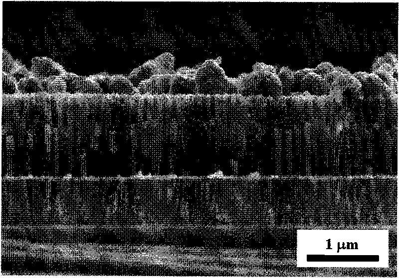
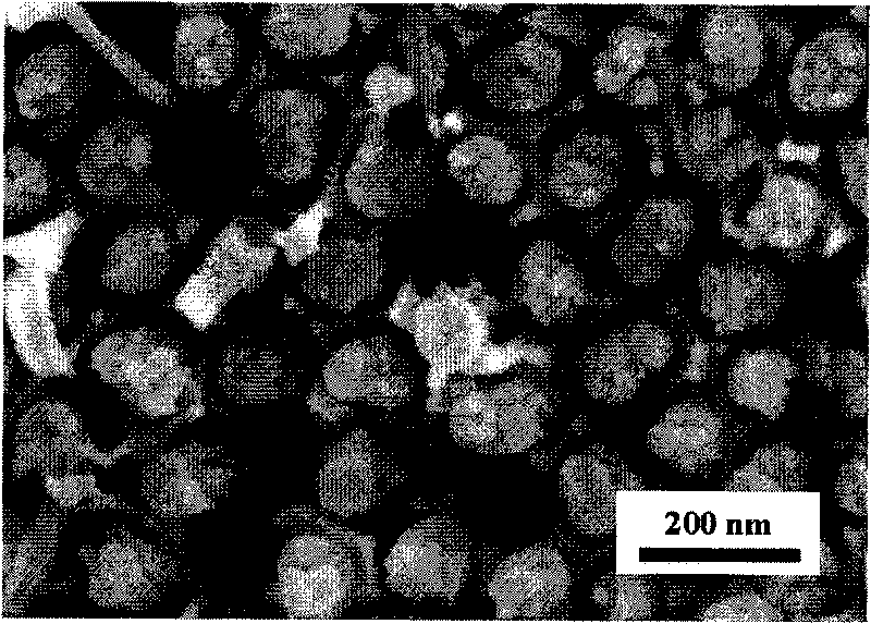
[0027] Embodiment 1, preparation copper indium selenium nanowire array

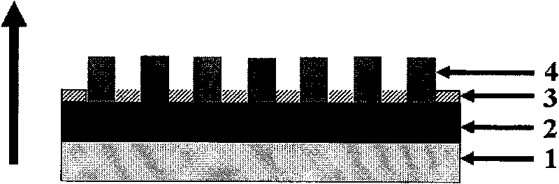
[0028] 1) With a silicon wafer with a thickness of 0.52 mm as the substrate, the Mo metal conductive layer was prepared by DC magnetron sputtering. The sputtering power was 120W, the sputtering pressure was 0.15Pa, and the sputtering time was 26 minutes. The thickness of the obtained Mo layer was 800nm.

[0029] 2) The Mo metal conductive layer covered with an ordered nano-template with a pore diameter of 50 nanometers, a distance between adjacent holes of 120 nanometers, and a thickness of 1200 nanometers is used as the cathode, and the material constituting the organic nano-template is an anodized aluminum template. The platinum sheet is the anode, and the saturated calomel electrode is the reference electrode, containing Cu 2+ 、In 3+ 、Se 4+ and Cl - , SO 4 2- Ionic aqueous solution as electrolyte solution, Cu 2+ 、In 3+ and Se 4+ The concentrations are 2 mmol / L, 2 mmol / L and 4 mmol / L respective...

Embodiment 2

[0032] Example 2, preparation of copper indium selenide nanowire array

[0033] 1) Using a silicon wafer with a thickness of 0.52 mm as the substrate, a W metal conductive layer was prepared by DC magnetron sputtering. The sputtering power was 120W, the sputtering pressure was 0.3Pa, and the sputtering time was 25 minutes. The thickness of the obtained W layer was 800nm.

[0034] 2) The W metal conductive layer covered with an ordered nano-template with a pore diameter of 90 nanometers, a distance between adjacent holes of 150 nanometers, and a thickness of 1600 nanometers is used as the cathode. The plate is the anode, and the saturated calomel electrode is the reference electrode, containing Cu 2+ 、In 3+ 、Se 4+ and Cl - , SO 4 2- An aqueous solution of ions is used as the electrolyte solution, Cu 2+ 、In 3+ and Se 4+ The concentrations are 5 mmol / L, 10 mmol / L and 10 mmol / L respectively, the control voltage is -0.6 volts, electrodeposited at room temperature for 20 mi...

Embodiment 3

[0037] Example 3, preparation of copper indium selenide nanowire array

[0038] 1) With a glass sheet with a thickness of 1.2 mm as the substrate, the Mo metal conductive layer was prepared by DC magnetron sputtering. The sputtering power was 80W, the sputtering pressure was 1.4Pa, and the sputtering time was 20 minutes. The thickness of the obtained Mo layer was 800nm.

[0039] 2) The Mo metal conductive layer covered with an ordered nano-template with a pore diameter of 90 nanometers, a distance between adjacent holes of 150 nanometers, and a thickness of 1600 nanometers is used as the cathode, and the material constituting the organic nano-template is an anodized aluminum template. The platinum sheet is the anode, and the saturated calomel electrode is the reference electrode, containing Cu 2+ 、In 3+ 、Se 4+ and Cl - , SO 4 2- Ionic aqueous solution as electrolyte solution, Cu 2+ 、In 3+ and Se 4+ The concentrations are 10 mmol / L, 10 mmol / L and 15 mmol / L respectively...


PUM

PropertyMeasurementUnit
thicknessaaaaaaaaaa
thicknessaaaaaaaaaa
thicknessaaaaaaaaaa

Abstract

The invention discloses a copper-indium-selenium nanowire array and a preparation method thereof. The method comprises the following steps: preparing a metal electrode layer on a glass or silicon slice substrate, using an ordered nano-template as growing mask to prepare the ordered nanowire structure copper-indium-selenium P-type absorbing layer material array on the metal electrode layer of the substrate through electrodeposition, and partly removing the template from top to bottom through chemical corrosion or physical etching method to expose the nanowire array. The array of the invention can be used to prepare the heterojunction solar cell with photoelectric translating performance.

Description

technical field [0001] The invention belongs to the technical field of thin-film solar cells, and relates to a copper indium selenium nanowire array and a preparation method and application thereof. Background technique [0002] As the energy issue has increasingly become a bottleneck restricting the development of the international community and China's economy, the development of solar energy technology has become one of the most important topics in the field of energy and materials research. It is imperative to develop low-cost, high-efficiency, and stable photovoltaic cells (M.A. Green, Progress in Photovoltaics: Research and Applications 9123-35 (2001)). Thin-film semiconductor photovoltaic cells are studied to reduce the manufacturing cost of battery components and promote the development of photovoltaic cell manufacturing industry (A.Barnett, A.Rothwarf, Thin-film solarcells: A unified analysis of their potential, IEEE Trans.Electron Devices 27 615 -630 (1980)). In ...

Claims


Application Information

Patent Timeline
Patent Type & Authority Applications(China)
IPC IPC(8): B82B3/00H01L31/18
CPCY02P70/50
Inventor 朱长飞张中伟刘伟丰
Owner UNIV OF SCI & TECH OF CHINA
Why Eureka
Try Eureka