Maskless method for preparing black silicon by deep reactive ion etching

A deep reactive ion, maskless technology, applied in the process of producing decorative surface effects, nanostructure manufacturing, manufacturing microstructure devices, etc., can solve the problems of low processing efficiency, small processing area, inapplicability, etc. Low cost and high efficiency

Active Publication Date: 2010-06-16
PEKING UNIV
View PDF0 Cites 47 Cited by
  • Summary
  • Abstract
  • Description
  • Claims
  • Application Information

AI Technical Summary

Problems solved by technology

However, the method based on chemical synthesis of Nil still has problems such as low processing efficiency, difficult control of processing quality (i.e. shape control and uniformity), and small processing area (millimeter level).
In addition, most of the above nanofabrication methods are only applicable to flat silicon wafer surfaces and not to non-planar microstructured surfaces, which limits their integration with other microfabrication processes.

Method used


Image

  • Maskless method for preparing black silicon by deep reactive ion etching
  • Maskless method for preparing black silicon by deep reactive ion etching
  • Maskless method for preparing black silicon by deep reactive ion etching

Examples


Embodiment Construction

[0022] In order to make the above objects, features and advantages of the present invention more comprehensible, the embodiments of the present invention will be further described in detail below in conjunction with the accompanying drawings and specific implementation methods.

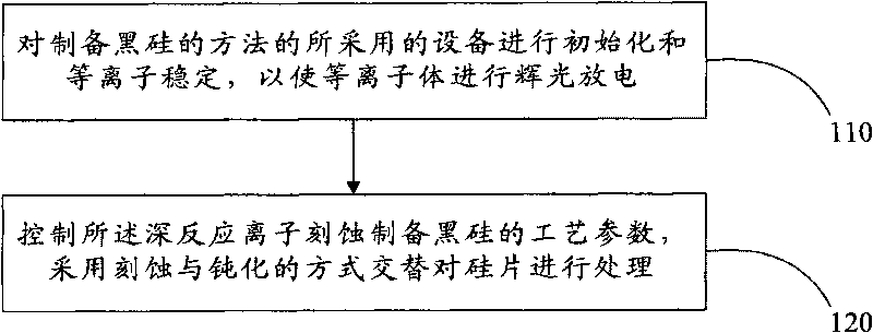
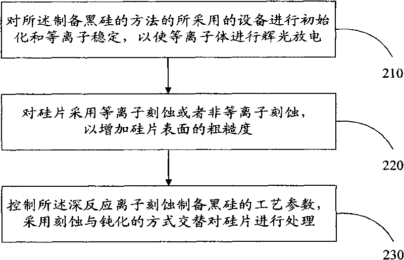
[0023] refer to figure 1 , figure 1 It is a flow chart of the steps of an embodiment of the method for preparing black silicon based on maskless deep reactive ion etching in the present invention, including the following steps:

[0024] Initialization and plasma stabilization step 110, performing initialization and plasma stabilization on the equipment used in the method for preparing black silicon, so as to make the plasma glow discharge;

[0025] The black silicon etching step 120 is to control the process parameters of the deep reactive ion etching to prepare black silicon, and alternately process the silicon wafer by means of etching and passivation; wherein, the parameters include: plasma gas fl...


PUM

PropertyMeasurementUnit
diameteraaaaaaaaaa
pore sizeaaaaaaaaaa

Abstract

The invention discloses a maskless method for preparing black silicon by deep reactive ion etching, which comprises the following steps: performing initialization and plasma stability on equipment adopted by the method for preparing the black silicon so as to make plasma perform glow discharge; and controlling technological parameters for preparing the black silicon by deep reactive ion etching, and adopting etching and passivating modes to alternately process a silicon chip, wherein the parameters comprise plasma gas flow, panel etching power, panel passivating power, coil power, and etching and passivating cycle and temperature. The maskless method directly performs plasma processing on the surface of the silicon chip, and can generate large-range high-intensity nanostructures on the surface of the silicon chip in case of no nano mask by adjusting and selecting proper etching technological parameters. Meanwhile, the method for preparing the black silicon has high efficiency and low cost, and can be integrated with other micro-fabrication technology.

Description

technical field [0001] The invention relates to a method for preparing a wafer-level black silicon surface in the field of micro-nano processing, in particular to a method for preparing black silicon based on maskless deep reactive ion etching. Background technique [0002] At present, nanostructure processing has been widely used in microfluidics, bioengineering, optical sensor devices and other fields. [0003] In micro-nanostructure processing, usually for different purposes, large-scale high-density uniform nanostructures (nanotips and nanoporous) are formed in substrates such as silicon wafers to increase the surface area to volume ratio. Nanostructures are formed by etching or deposition growth and a combination of various processes. For example, nano-lithography technology is used to define a nano-mask on a silicon wafer substrate, and then a dry etching technology is used to form a nano-pillar (nanopillar). Typically, forming nanostructures by etching requires firs...

Claims


Application Information

Patent Timeline
Patent Type & Authority Applications(China)
IPC IPC(8): B81C1/00B82B3/00
Inventor 张海霞孙广毅高天乐
Owner PEKING UNIV
Why Eureka
Try Eureka