LDMOS (Laterally Diffused Metal Oxide Semiconductor) transistor, semiconductor device and manufacture method thereof

A technology of transistors and semiconductors, applied in semiconductor/solid-state device manufacturing, electrical components, circuits, etc., can solve the problems of narrow depletion region, high cost, and affecting actual use, so as to reduce turn-on resistance, improve withstand voltage, and high The effect of breakdown voltage

Active Publication Date: 2010-06-16
SEMICON MFG INT (SHANGHAI) CORP
View PDF1 Cites 16 Cited by
  • Summary
  • Abstract
  • Description
  • Claims
  • Application Information

AI Technical Summary

Problems solved by technology

[0007] In this technical solution, the P-region 204 is used as the drift region of the drain 209, and the effective channel length is figure 2 As shown in DLL, under the gate voltage, a reverse-biased diode is formed between the P-region 204 and the P-region 204, the depletion region is narrow, and the withstand voltage of the LDMOS transistor is low, resulting in the I-V of the LDMOS transistor A snapback phenomenon will app

Method used


Image

  • LDMOS (Laterally Diffused Metal Oxide Semiconductor) transistor, semiconductor device and manufacture method thereof
  • LDMOS (Laterally Diffused Metal Oxide Semiconductor) transistor, semiconductor device and manufacture method thereof
  • LDMOS (Laterally Diffused Metal Oxide Semiconductor) transistor, semiconductor device and manufacture method thereof

Examples


Embodiment Construction

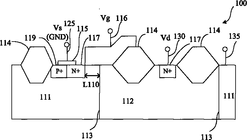
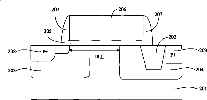
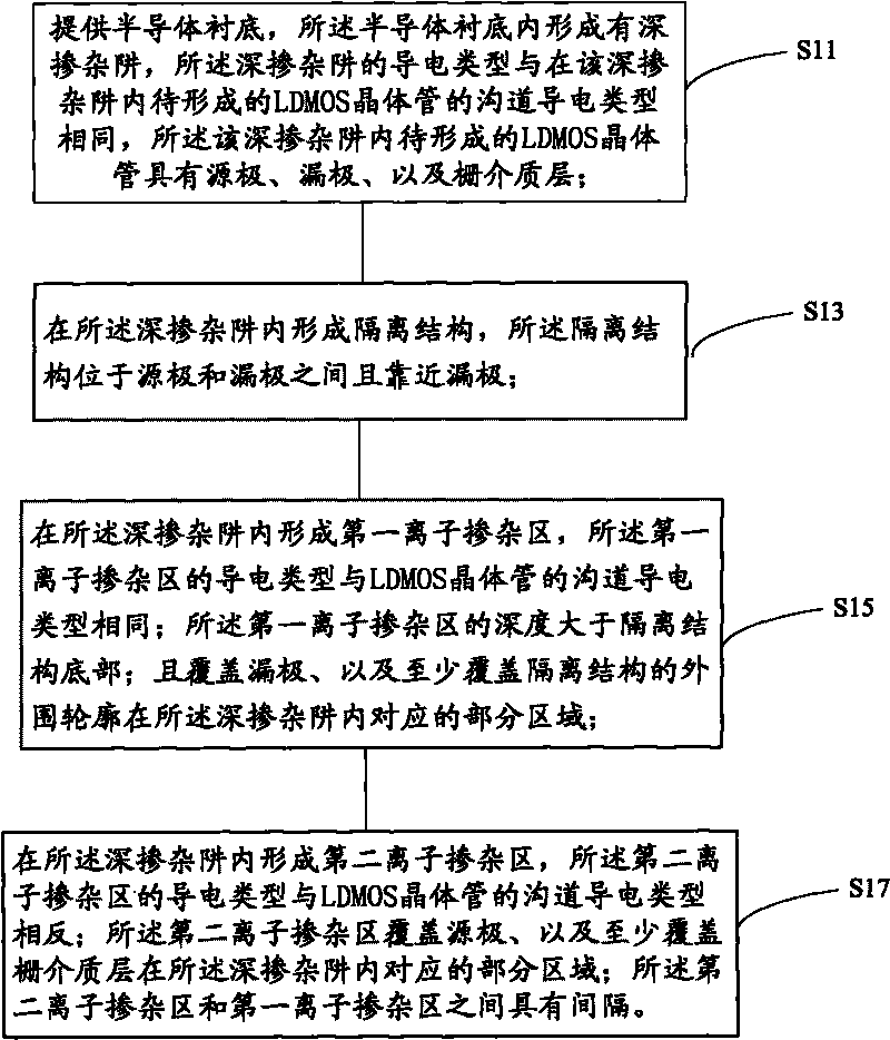
[0042] In the present invention, a deep doped well of the same conductivity type as the channel of the LDMOS transistor to be formed is formed in the semiconductor substrate, and then a first ion-doped region and a second ion-doped region isolated from each other are formed in the deep doping , the conductivity type of the first ion-doped region is the same as that of the channel, the conductivity type of the second ion-doped region is opposite to that of the channel, the channel of the LDMOS transistor is the corresponding second ion-doped region under the gate dielectric layer, and the channel Shorter, under the gate voltage, a reverse-biased diode is formed between the deep doped well and the first ion-doped region and the second ion-doped region, and the region is completely depleted before breakdown, and a higher High breakdown voltage, that is, the fast return phenomenon in the I-V curve of the LDMOS transistor shifts to the right, which improves the withstand voltage of ...


PUM


Abstract

The invention relates to an LDMOS (Laterally Diffused Metal Oxide Semiconductor) transistor, a semiconductor device and a manufacture method thereof, wherein the manufacture method of the LDMOS transistor comprises the steps of: forming a deep-doped well in a semiconductor substrate; forming an isolation structure in the deep-doped well, wherein the isolation structure is arranged between a source electrode and a drain electrode and is close to the drain electrode; forming a first ion doping area in the deep-doped well; and forming a second ion doping area in the deep-doped well, wherein a space is reserved between the first ion doping area and the second ion doping area. By forming the deep-doped well which has the same channel conduction type with the LDMOS transistor to be formed in the semiconductor substrate, the invention can obtain higher breakdown voltage.

Description

technical field [0001] The invention relates to the technical field of semiconductors, in particular to LDMOS transistors, semiconductor devices with LDMOS transistors and manufacturing methods thereof. Background technique [0002] In the development of power integrated circuits, the single-chip process developed to integrate power switches and control circuits, especially the lateral double diffusion MOS (lateral double diffusion MOS, LDMOS) process is a mainstream trend. The LDMOS process is planar diffusion on the surface of the semiconductor substrate to form the main lateral current path. Since LDMOS is manufactured in a typical IC process, the control circuit and LDMOS can be integrated on a monolithic power IC. LDMOS The process uses reduced surface electric field (RESURE) technology and low-thickness epitaxy (EPI) or N-type well region (N-well), which can achieve the goals of high voltage and low on-resistance. [0003] The LDMOS device is a field-effect transisto...

Claims


Application Information

Patent Timeline
IPC IPC(8): H01L21/336H01L21/8234
Inventor 郑大燮王东立陈德艳陈良成崔崟
Owner SEMICON MFG INT (SHANGHAI) CORP
Why Eureka
Try Eureka