Method for preparing solar array electrode by electro-brush plating

A silicon solar cell and array electrode technology, which is applied in the manufacture of circuits, electrical components, and final products, can solve the problems of reduced effective area for absorbing solar energy and reduced conversion efficiency, and achieves small investment, reduced contact resistance, and fast plating speed Effect

Active Publication Date: 2010-07-28
SOUTH CHINA NORMAL UNIVERSITY
View PDF1 Cites 18 Cited by
  • Summary
  • Abstract
  • Description
  • Claims
  • Application Information

AI Technical Summary

Problems solved by technology

However, there are currently the following problems in this process: the obtained grid-shaped array electrodes will cover about 6-10% of the surface area, which reduces the effective area for absorbing solar energy, thereby reducing the conversion efficiency; Array electrodes with higher aspect ratio

Method used


Image

  • Method for preparing solar array electrode by electro-brush plating
  • Method for preparing solar array electrode by electro-brush plating
  • Method for preparing solar array electrode by electro-brush plating

Examples


Embodiment 1

[0033] (1) Protective film coating: coating a layer of phenolic novolac on the surface of the silicon semiconductor coated with a silicon nitride anti-reflection layer as a protective film; the silicon semiconductor has a p / n junction;

[0034] (2) Laser grooving: engraving array grooves by laser on the surface of the silicon semiconductor coated with a protective film;

[0035] (3) Surface activation treatment: After the silicon semiconductor with the array groove engraved is cleaned by fatty alcohol polyoxyethylene ether sodium sulfate with a mass percentage concentration of 5%, the groove is treated in a HF hydrochloric acid solution with a mass percentage concentration of 5%. Activation was carried out for 5 minutes to obtain a pretreated silicon semiconductor;

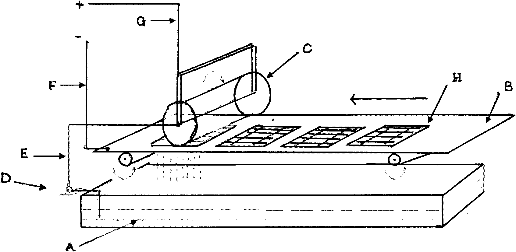
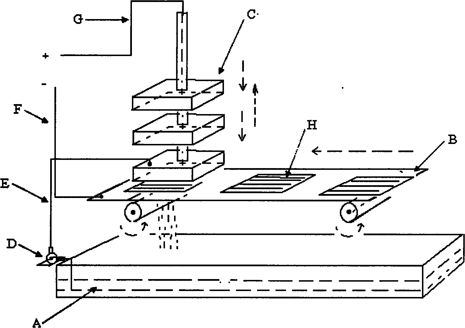
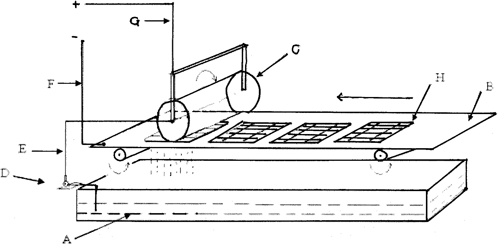
[0036] (4) Brush plating: use a conventional electroplating power supply, use the negative electrode of the power supply to connect the pretreated silicon semiconductor, connect the positive electrode of the power...

Embodiment 2

[0040](1) protective film coating: coating a layer of alkyd varnish on the surface of a silicon semiconductor coated with a porous silicon dioxide anti-reflection layer as a protective film; the silicon semiconductor has a p / n junction;

[0041] (2) Laser grooving: engraving array grooves by laser on the surface of the silicon semiconductor coated with a protective film;

[0042] (3) Surface activation treatment: After cleaning the silicon semiconductor with the array grooves with a mass percentage concentration of 0.5% sodium dodecylbenzene sulfonate, the silicon semiconductor with a mass percentage concentration of 5% HBF 4 Activate the groove for 5 minutes in a hydrochloric acid solution to obtain a pretreated silicon semiconductor;

[0043] (4) Brush plating: use a conventional electroplating power supply, use the negative electrode of the power supply to connect the pretreated silicon semiconductor, connect the positive electrode of the power supply to a mobile plating pe...

Embodiment 3

[0047] (1) protective film coating: coating a layer of nitro varnish as a protective film on the surface of a silicon semiconductor coated with a titanium dioxide anti-reflection layer; the silicon semiconductor has a p / n junction;

[0048] (2) Laser grooving: engraving array grooves by laser on the surface of the silicon semiconductor coated with a protective film;

[0049] (3) Surface activation treatment: After the silicon semiconductor with the array grooves is cleaned by sodium dodecyl sulfate with a mass percentage concentration of 2%, the NH 4 HF 2 Activate the groove for 2 minutes in a hydrochloric acid solution to obtain a pretreated silicon semiconductor;

[0050] (4) Brush plating: use a conventional electroplating power supply, use the negative pole of the power supply to connect the pretreated silicon semiconductor, connect the positive pole of the power supply to a pictographic plating pen filled with plating solution, turn on the power supply, and place the pla...


PUM


Abstract

The invention discloses a method for preparing a silicon solar array electrode by electro-brush plating, which comprises the steps of: (1) coating of a protective film; (2) laser grooving; (3) surface activation treatment; (4) electro-brush plating: a general electroplating power supply is adopted; a cathode of the power supply is connected with a pretreated silicon semiconductor; an anode of the power supply is connected with an plating pen immersed with a plating solution; the power supply is started; the electro-brush plating is carried out on the plating pen on the surface of the pretreated silicon semiconductor; and the plating pen is a mobile plating pen or a pictographic plating pen; and (5) the removal of the protective film. The invention obviously enhances the production efficiency by adopting the electro-brush plating and realizes the preparation of the array electrode within a shorter time; the prepared electrode is uniform and bright; at the same time, the electroplating bath solution has easy maintenance; the electrode has high bonding strength with a base body and plating layers have high bonding force, thereby reducing contact resistance between the base body and a conducting wire; and the invention has good automatic degree, high electroplating speed, simple technological operation, easy mastery, relatively lower cost, high efficiency and less required tooling equipment.

Description

technical field [0001] The invention belongs to the field of solar cell preparation, in particular to a method for preparing silicon solar cell array electrodes by electric brush plating. Background technique [0002] At present, there is only one method for commercially producing silicon solar cell array electrodes, that is, screen printing silver paste to form array electrodes. However, there are currently the following problems in this process: the obtained grid-like array electrode will cover about 6% to 10% of the surface area, which reduces the effective area for absorbing solar energy, thereby reducing the conversion efficiency; Array electrodes with higher aspect ratios. Contents of the invention [0003] In order to solve the deficiencies in the above-mentioned prior art, the primary purpose of the present invention is to provide a method for preparing silicon solar cell array electrodes by brush plating. [0004] Another object of the present invention is to pr...

Claims


Application Information

Patent Timeline
Patent Type & Authority Applications(China)
IPC IPC(8): H01L31/18H01L31/0224C25D5/06
CPCY02P70/50
Inventor 莫烨强黄启明吴飞黄美玲李伟善
Owner SOUTH CHINA NORMAL UNIVERSITY
Why Eureka
Try Eureka