Hole punching device for carbon dioxide buffer silicon wafer

A carbon dioxide and hole punching device technology, applied in the field of silicon wafer etching, can solve the problems of poor line width control, device damage, low sidewall smoothness, etc., and achieves improved development and development, overcoming expensive equipment and good sidewall smoothness. Effect

Inactive Publication Date: 2010-11-10
INST OF MICROELECTRONICS CHINESE ACAD OF SCI
View PDF0 Cites 0 Cited by
  • Summary
  • Abstract
  • Description
  • Claims
  • Application Information

AI Technical Summary

Problems solved by technology

Plasma chemical etching is isotropic, so line width control is relatively poor
Although physical etching is anisotropic and the etching rate is fast, the selectivity is poor, and the elements removed by bombardment are non-volatile, which are easy to deposit on the surface of the silicon wafer, causing particle pollution
In addition, the charge generated by the non-uniform plasma can cause the failure of sensitive devices on the silicon wafer
Plasma etching equipment is expensive, the etching selectivity is poor, the sidewall is not smooth, and it is easy to cause device damage, so it is not suitable for next-generation semiconductor silicon etching

Method used


Image

  • Hole punching device for carbon dioxide buffer silicon wafer
  • Hole punching device for carbon dioxide buffer silicon wafer
  • Hole punching device for carbon dioxide buffer silicon wafer

Examples


Embodiment Construction

[0019] In order to make the object, technical solution and advantages of the present invention clearer, the present invention will be described in further detail below in conjunction with specific embodiments and with reference to the accompanying drawings.

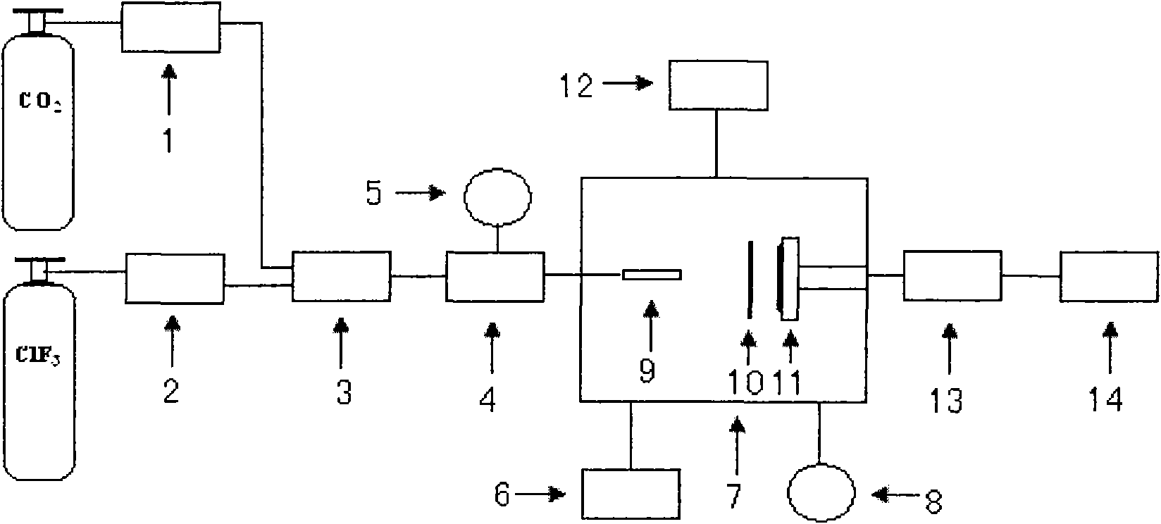
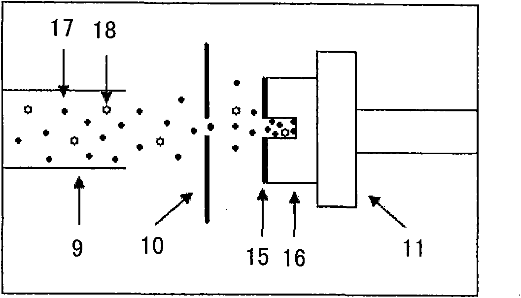
[0020] The carbon dioxide buffered silicon chip punching device provided by the present invention adopts chlorine trifluoride as the etching reaction gas, and the carbon dioxide acts as a buffering regulator. Chlorine trifluoride etching of silicon wafers is carried out in a plasma-free environment. Compared with traditional RIE and ICP etching, this etching system has simple equipment, faster etching rate, and can drill oblique holes at any angle. , and the steepness and smoothness of the side wall are greatly improved. Carbon dioxide is used as a buffer agent, on the one hand, to adjust the gas mixing ratio in the gas path, and improve safety; on the other hand, carbon dioxide is easy to form dry ice when it is rapidly ...


PUM


Abstract

The invention relates to a hole punching device for a carbon dioxide buffer silicon wafer, which comprises a carbon dioxide flow controller, a chlorine triflouride flow controller, a mixer, a reducing valve, a pressure gage, a vacuum pump, a vacuum chamber, a vacuum chamber pressure gage, a sprayer, a masking plate, a silicon water bracket, a vacuum chamber temperature control device, a backward stage pump and a tail gas treating device. The reducing valve, the vacuum pump, the vacuum chamber pressure gage, the vacuum chamber temperature control device, and the backward stage pump are respectively connected with the vacuum chamber. Carbon dioxide gas enters the mixer through the carbon dioxide flow controller and chlorine triflouride gas enters the mixer through the chlorine triflouride flow controller. Carbon dioxide gas and chlorine triflouride gas are mixed in the mixer and the mixed gas enters the vacuum chamber through the reducing valve and the sprayer in sequence and is masked and adjusted by means of beam convergence by the masking plate to punch holes on the silicon wafer on the silicon wafer bracket. The invention has the advantages of simple device, rapid etching speed, good smoothness of the lateral wall and great selection ratio and realizes hole punching for the silicon wafer.

Description

technical field [0001] The invention relates to the technical field of silicon wafer etching in semiconductor technology, in particular to a carbon dioxide buffer silicon wafer drilling device. Background technique [0002] In the MEMS manufacturing process, deep etching of silicon is a commonly used process. The traditional dry etching technology is plasma etching, such as RIE, ICP. Etching is achieved through chemical and physical actions. Plasma chemical etching is isotropic, so line width control is relatively poor. Although physical etching is anisotropic and has a fast etching rate, its selectivity is poor, and the elements removed by bombardment are non-volatile and easily deposited on the surface of the silicon wafer, causing particle contamination. In addition, charges generated by non-uniform plasmas can cause failure of sensitive devices on silicon wafers. Plasma etching equipment is expensive, the etching selectivity is poor, the sidewall smoothness is not hi...

Claims


Application Information

Patent Timeline
Patent Type & Authority Applications(China)
IPC IPC(8): C23F1/12
Inventor 景玉鹏惠瑜
Owner INST OF MICROELECTRONICS CHINESE ACAD OF SCI
Why Eureka
Try Eureka