Two-dimensional and double-cycle ordered structure array and preparation method thereof

An ordered structure, double-period technology, applied in nanostructure manufacturing, microstructure technology, microstructure devices, etc., can solve problems such as time-consuming, inability to obtain double-period ordered structure arrays, difficulty in controlling the size of silver branches, etc., to achieve The effect of excellent performance

Inactive Publication Date: 2010-11-24
HEFEI INSTITUTES OF PHYSICAL SCIENCE - CHINESE ACAD OF SCI
View PDF1 Cites 25 Cited by
  • Summary
  • Abstract
  • Description
  • Claims
  • Application Information

AI Technical Summary

Problems solved by technology

However, this preparation method has shortcomings. First of all, it is too specific, and can only produce silver dendritic structure arrays in the periodically arranged zinc oxide inverse opal structure templates, but cannot obtain structures composed of other shapes and materials. The dual-period ordered structure array; secondly, the preparation method is more complicated and time-consuming, and it is difficult to control the size of the primary template unit or the size of the silver branch

Method used


Image

  • Two-dimensional and double-cycle ordered structure array and preparation method thereof
  • Two-dimensional and double-cycle ordered structure array and preparation method thereof
  • Two-dimensional and double-cycle ordered structure array and preparation method thereof

Examples


Embodiment 1

[0028] The concrete steps of preparation are:

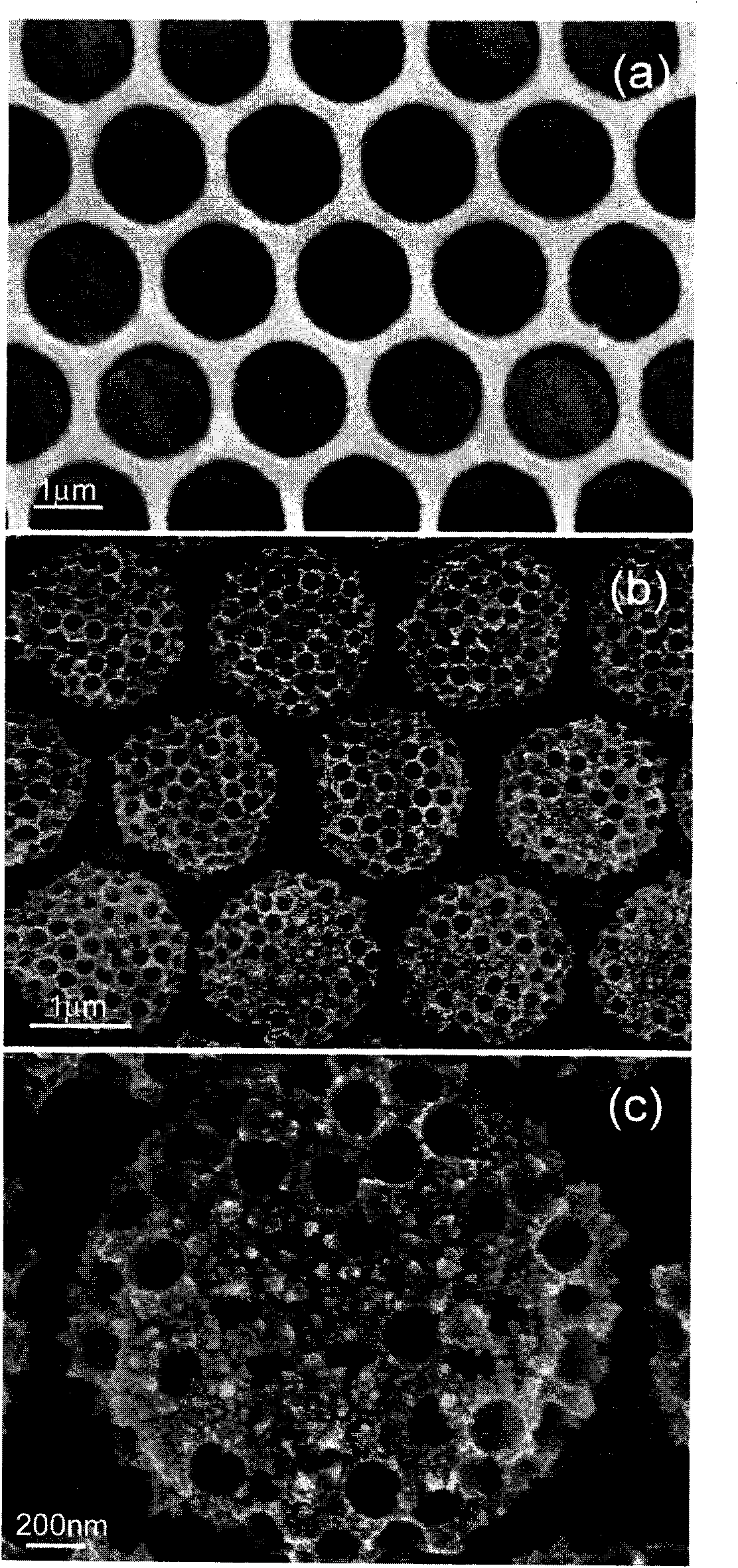
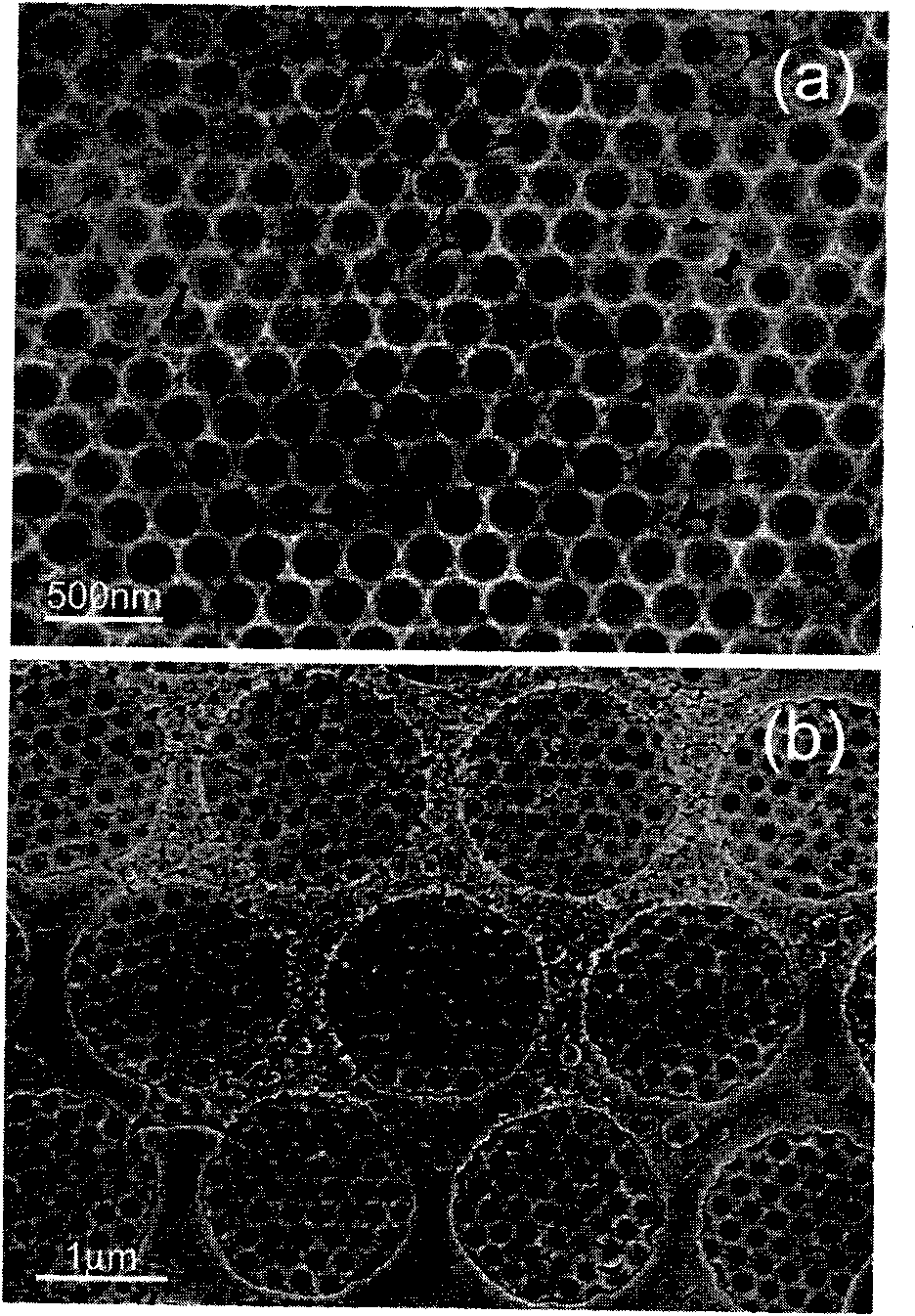
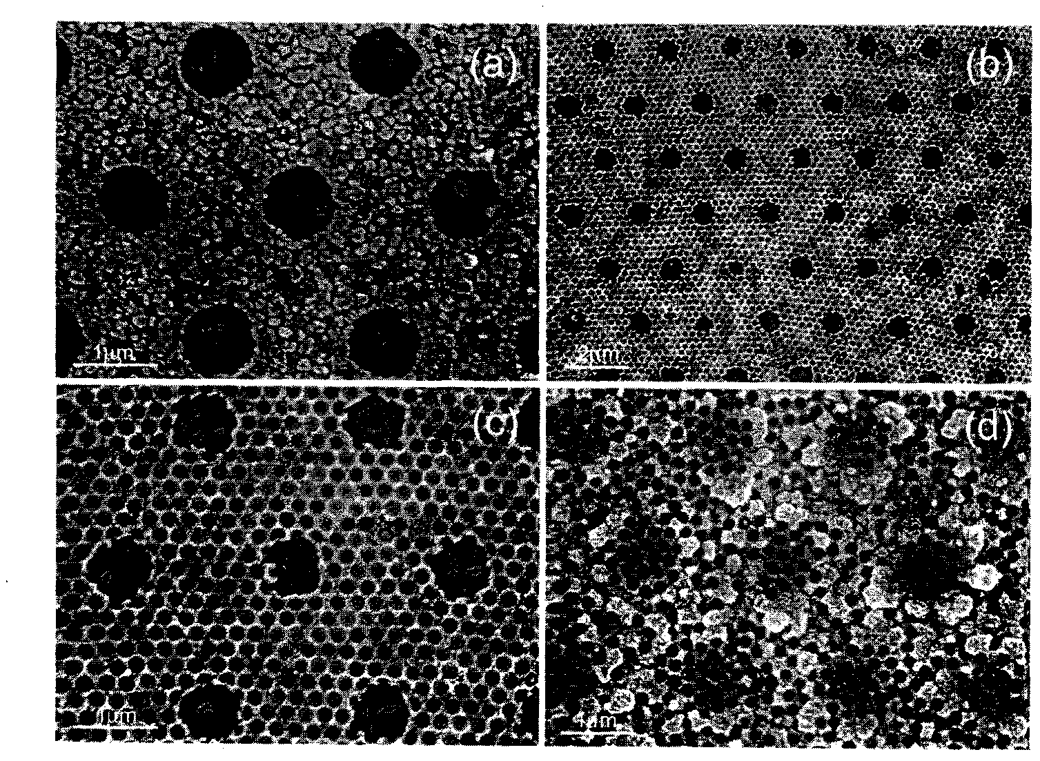
[0029] First place the conductive substrate with a single-layer colloidal crystal template with a spherical diameter of 1800nm ​​on it and heat it for 18 minutes at a temperature of 80°C, then drop an aluminum nitrate solution with a concentration of 0.2M on it, and place it Rotate for 35 minutes at a rotational speed of 100r / min; wherein, the conductive substrate is conductive glass. Next, it was first heated at 110°C for 1.2h, then immersed in dichloromethane solvent to remove polystyrene colloidal balls, and then heated at 140°C for 9h to obtain an approximate figure 1 a. Figure 4 a Al2O3 ordered hole array attached to a conductive substrate shown in II. Afterwards, polystyrene colloidal spheres with a diameter of 180 nm were self-assembled into the holes of the ordered hole array of Al2O3 by spin-coating method to obtain an approximate Figure 4 The complex array shown in aIII; wherein, the rotation speed of the conductiv...

Embodiment 2

[0035] The concrete steps of preparation are:

[0036] First place the conductive substrate with a single-layer colloidal crystal template with a spherical diameter of 1900nm on it and heat it for 17 minutes at a temperature of 90°C, then drop an aluminum nitrate solution with a concentration of 0.4M on it, and place it Rotate for 33 minutes at a rotational speed of 150r / min; wherein, the conductive substrate is conductive glass. Next, it was first heated at 115°C for 1.1h, then immersed in dichloromethane solvent to remove polystyrene colloidal balls, and then heated at 145°C for 8.5h to obtain an approximate figure 1 a. Figure 4 Al2O3 ordered hole array attached to a conductive substrate shown in aII. Afterwards, polystyrene colloidal spheres with a diameter of 190 nm were self-assembled into the pores of the Al2O3 ordered pore array by spin-coating method to obtain an approximate Figure 4 The composite array shown in aIII; wherein, the rotation speed of the conductive ...

Embodiment 3

[0042] The concrete steps of preparation are:

[0043] First place the conductive substrate with a single-layer colloidal crystal template with a spherical diameter of 2000nm on it and heat it for 16min at a temperature of 100°C, then drop an aluminum nitrate solution with a concentration of 0.6M on it, and place it Rotate at a rotational speed of 200r / min for 30min; wherein, the conductive substrate is conductive glass. Next, it was first heated at 120°C for 1 hour, then immersed in dichloromethane solvent to remove polystyrene colloidal balls, and then heated at 150°C for 8 hours to obtain the following: figure 1 a. Figure 4 Al2O3 ordered hole array attached to a conductive substrate shown in aII. Afterwards, polystyrene colloidal spheres with a diameter of 200 nm were self-assembled into the holes of the Al2O3 ordered hole array by the spin coating method to obtain the following: Figure 4 The composite array shown in aIII; wherein, the rotation speed of the conductive ...


PUM

PropertyMeasurementUnit
pore sizeaaaaaaaaaa
diameteraaaaaaaaaa
diameteraaaaaaaaaa

Abstract

The invention discloses a two-dimensional and double-cycle ordered structure array and a preparation method thereof. The array is an ordered porous film consisting of metals in a microparticle hole shape and a nanometer hole shape and arranged on a conductive substrate, the nanometer hole in the film is located in the microparticle hole and is in a stacking shape, or the nanometer hole is a single layer and is located at the bottom surface or the external surface of the microparticle hole or covers the internal surface and the external surface thereof, the diameter of the microparticle hole is 1,800-2,200 nm, and the diameter of the thenanometer hole is 180-220 nm. The method comprises the following steps of: firstly, self-assembling by using a polystyrene colloidal ball of one diameter in combination with a solution impregnating method or an electrodepositing method to obtain the ordered hole array of a bowl-shaped metal attached to the conductive substrate; and then self-assembling thereon by utilizing polystyrene colloidal of another diameter in combination with the electrodepositing method to prepare the two-dimensional and double-cycle ordered structure arrays in four structures. The product thereof has the characteristics of a macro-scale system, the preparation method has universality, and the two-dimensional double-cycle and ordered structure array consisting of other conductive materials can be prepared by the method.

Description

technical field [0001] The invention relates to an ordered structure array and a preparation method thereof, in particular to a two-dimensional double-period ordered structure array and a preparation method thereof. Background technique [0002] Macro-scale nanostructure arrays not only have the inherent properties of the nanomaterials that make up the array units, but also produce some new properties that isolated units do not have due to the coupling effect between the units. For example, through the study of surface-enhanced Raman scattering (SERS) active substrates, it was found that the contribution of the coupling effect between nanostructure units to SERS enhancement is much greater than the geometric superposition of individual unit contributions. In addition, since the macro-scale system contains a large number of constituent units, this will greatly enhance the signal released by the system, which is conducive to the collection and application of the signal during ...

Claims


Application Information

Patent Timeline
Patent Type & Authority Applications(China)
IPC IPC(8): B81B7/04B82B1/00B81C1/00B82B3/00
Inventor 段国韬蔡伟平罗媛媛吕方景
Owner HEFEI INSTITUTES OF PHYSICAL SCIENCE - CHINESE ACAD OF SCI
Why Eureka
Try Eureka