Structure of quantum cascade detector

A quantum cascade and detector technology, applied in semiconductor devices, electrical components, circuits, etc., can solve problems such as low detection rate and operating temperature, large dark current noise, and power consumption

Inactive Publication Date: 2010-11-24
INST OF SEMICONDUCTORS - CHINESE ACAD OF SCI
View PDF1 Cites 7 Cited by
  • Summary
  • Abstract
  • Description
  • Claims
  • Application Information

AI Technical Summary

Problems solved by technology

Since the applied electric field of the photoconductive detector will introduce a relatively large dark current, it is easy to saturate the readout circuit capacitance of the infrared focal plane array and bring relatively large dark current noise and power consumption, so no external electric f

Method used


Image

  • Structure of quantum cascade detector
  • Structure of quantum cascade detector
  • Structure of quantum cascade detector

Examples


Embodiment Construction

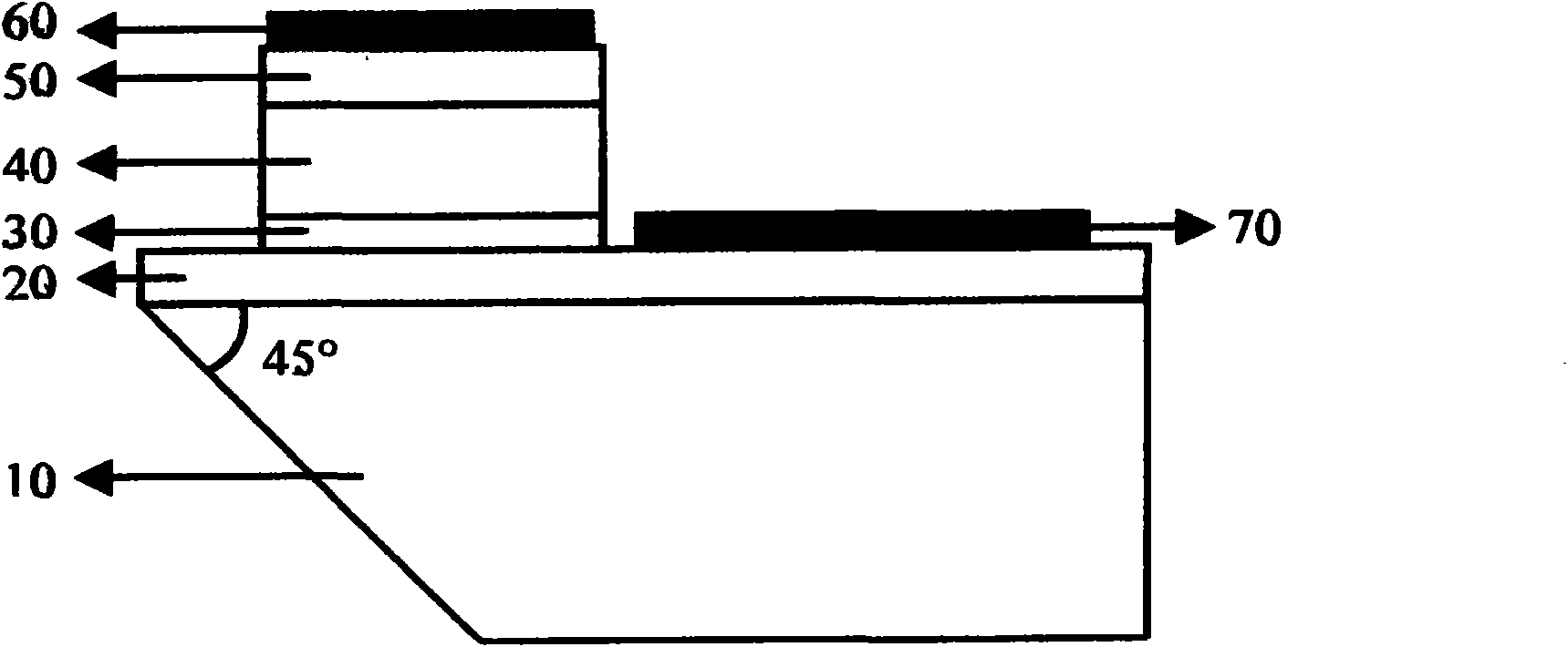
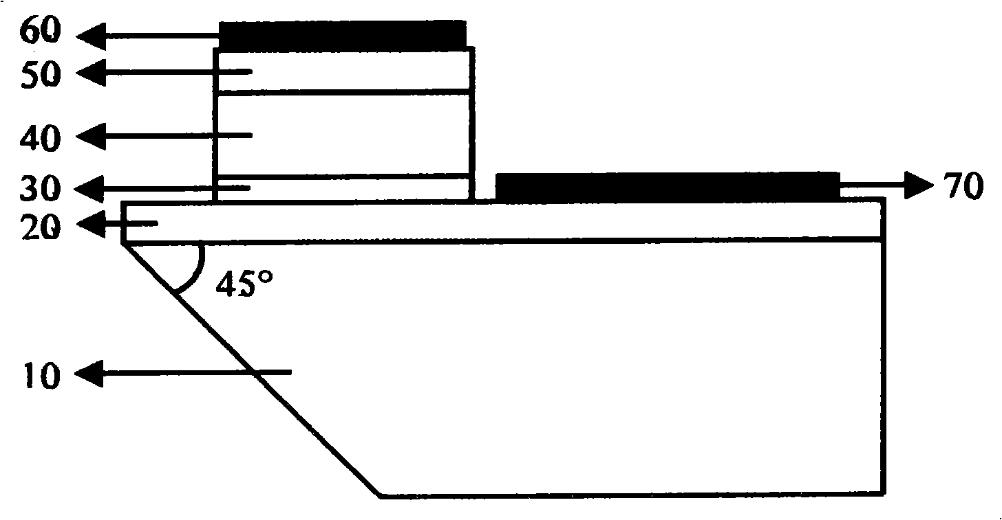
[0023] see figure 1 As shown, the present invention provides a quantum cascade detector structure, comprising:

[0024] A substrate 10, the material of the substrate 10 is gallium arsenide or indium phosphide, and one side of the bottom surface of the substrate 10 forms a 45-degree slope, which is due to the fact that the sub-band transition of the quantum cascade detector can only Absorb the TM polarization component of the incident light, and the incident light is incident perpendicular to the 45-degree inclined plane;

[0025] A lower ohmic contact layer 20, the lower ohmic contact layer 20 is fabricated on the substrate 10, the lower ohmic contact layer 20 is doped at a high concentration to realize ohmic contact with the electrode material, and the material of the lower ohmic contact layer 20 is arsenic Gallium or indium gallium arsenic, doped with silicon doped, the concentration is generally 1×10 18 cm -3 ;

[0026] A barrier isolation layer 30, the barrier isolatio...


PUM


Abstract

The invention provides the structure of a quantum cascade detector, which comprises a substrate, a lower ohmic contact layer, a barrier isolation layer, a multi-cycle active region structure layer, an upper ohmic contact layer, an upper electrode and a lower electrode, wherein the lower ohmic contact layer is arranged on the substrate and is used for carrying out the high-concentration doping process to achieve the ohmic contact with electrode materials; the barrier isolation layer is arranged at the middle part of the lower ohmic contact layer to form a table top all around the lower ohmic contact layer, wherein the barrier isolation layer is not doped; the multi-cycle active region structure layer is arranged on the barrier isolation layer and constitutes the core part of the detector for detecting light current; the upper ohmic contact layer is arranged on the multi-cycle active region structure layer and is used for carrying out the high-concentration doping process to achieve the ohmic contact with the electrode materials; the upper electrode is prepared on the upper ohmic contact layer; and the lower electrode is prepared on the table top all around the lower ohmic contact layer.

Description

technical field [0001] The invention relates to semiconductor photoelectric detection technology, in particular to a quantum cascade detector structure. Background technique [0002] Infrared detectors are a class of detectors with important application value. Their applications cover various fields of military, medical, scientific research and daily life. It is of great significance to continuously explore and develop new and high-performance infrared detectors. At present, the detectors used as infrared focal plane detectors are mainly photoconductive HgCdTe infrared detectors or photoconductive quantum well infrared detectors. Since the applied electric field of the photoconductive detector will introduce a relatively large dark current, it is easy to saturate the readout circuit capacitance of the infrared focal plane array and bring relatively large dark current noise and power consumption, so no external electric field is required, and it works by photovoltaic effect ...

Claims


Application Information

Patent Timeline
IPC IPC(8): H01L31/101
Inventor 孔宁刘俊岐李路刘峰奇王利军王占国
Owner INST OF SEMICONDUCTORS - CHINESE ACAD OF SCI
Why Eureka
Try Eureka