Multi-beam semiconductor laser interference nanoimprinting technology and system

A technology of laser interference and nano-lithography, which is applied in the direction of semiconductor lasers, lasers, and laser components, etc., can solve the problems of difficulty in adjusting the incident angle and phase of coherent beams in the beam splitting system, large volume of lasers, and low flexibility.

Inactive Publication Date: 2010-12-15
CHANGCHUN UNIV OF SCI & TECH
View PDF5 Cites 28 Cited by
  • Summary
  • Abstract
  • Description
  • Claims
  • Application Information

AI Technical Summary

Problems solved by technology

[0003] The current laser interference lithography method is mainly based on the traditional lithography system design idea, the laser used is relatively large in size, and the optical path design of the beam splitting system is also very complicated, which makes the complexity and price of the entire lithography system Very high, not only has no portability at all, but also greatly limits the application range of the system
For example, in a traditional photolithography system, the la

Method used


Image

  • Multi-beam semiconductor laser interference nanoimprinting technology and system
  • Multi-beam semiconductor laser interference nanoimprinting technology and system

Examples


Embodiment Construction

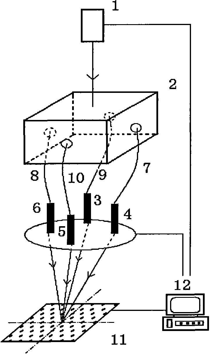
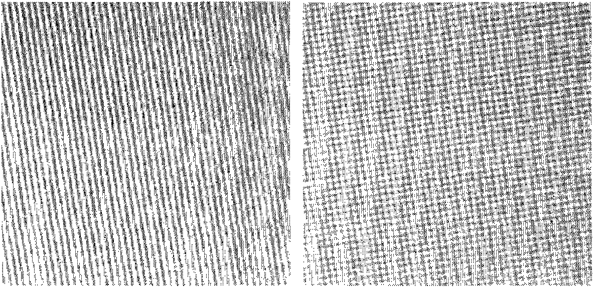
[0018] Such as figure 1 As shown, the semiconductor laser interference nanolithography system adopted in the present invention includes a semiconductor laser (wavelength 405nm) 1, a fiber coupling beam splitter 2, a beam shaping coupler and its control displacement components 3 to 6, laser fibers 7 to 10, three-dimensional Nanometer displacement and 90° horizontal rotation sample platform 11, computer 12. The laser light emitted by the computer-controlled semiconductor laser 1 is split by the beam-splitting coupler 2, and the separated four beams of coherent light are respectively transmitted by the laser fibers 7 to 10, and the four beams pass through the beam shaping coupler and its control components 3 to 6 Finally, the surface of the sample platform 11 is finally interfered, exposed on the sample coated with photoresist to form a periodic interference pattern, and the corresponding material surface micro-nano structure is obtained by etching. figure 2 are one-dimensional...


PUM


Abstract

The invention discloses multi-beam semiconductor laser interference nanoimprinting technology and system which adopt the following principle that the required two or more bundles of coherent lights can be obtained by using semiconductor pulse laser through beam splitting, the coherent lights are subjected to coupling, beam expansion and reshaping and redistributed on the surface of material by using the light intensity in an interference field to form a periodical interference pattern. When the system is used for imprinting, a photosensing material can be directly subjected to the interference exposure and then etching without masking. By using an optical fiber beam splitting device as a light splitter, the complicity of a light path is greatly reduced, and the system is more stable and reliable; in addition, the selection from two light beams to a plurality of light beams is more flexible and convenient.

Description

technical field [0001] The invention relates to a micro-nano surface structure manufacturing technology and system, in particular to a simple and low-cost multi-beam semiconductor laser interference nanolithography technology and system, which can be widely used in information storage, advanced manufacturing, new energy and new Materials and other technology fields. technical background [0002] The principle of laser interference lithography is to use the energy distribution of the interference pattern array generated by the interference of two or more laser beams to interact with materials to create surface micro-nano structures. The interference pattern can be an energy distribution of a line (two-beam interference) or a two-dimensional array of spots (multi-beam interference). This technology has the advantage of continuously adjustable feature size, shape and period from nanometers to micrometers. In air, the minimum period can be close to 1 / 2 wavelength. Laser inter...

Claims


Application Information

Patent Timeline
IPC IPC(8): G03F7/20H01S5/00
Inventor 徐佳王作斌翁占坤宋正勋胡贞刘兰娇侯煜潘海艳
Owner CHANGCHUN UNIV OF SCI & TECH
Why Eureka
Try Eureka