Process for producing laminate comprising Al-based group III nitride single crystal layer, laminate produced by the process, process for producing Al-based group III nitride single crystal substrate using the laminate, and aluminum nitride single cry
A single crystal substrate and laminated substrate technology, applied in chemical instruments and methods, crystal growth, single crystal growth, etc., can solve problems such as poor thermal expansion coefficient, crack cracking, deformation, etc.
- Summary
- Abstract
- Description
- Claims
- Application Information
AI Technical Summary
Problems solved by technology
Method used
Image

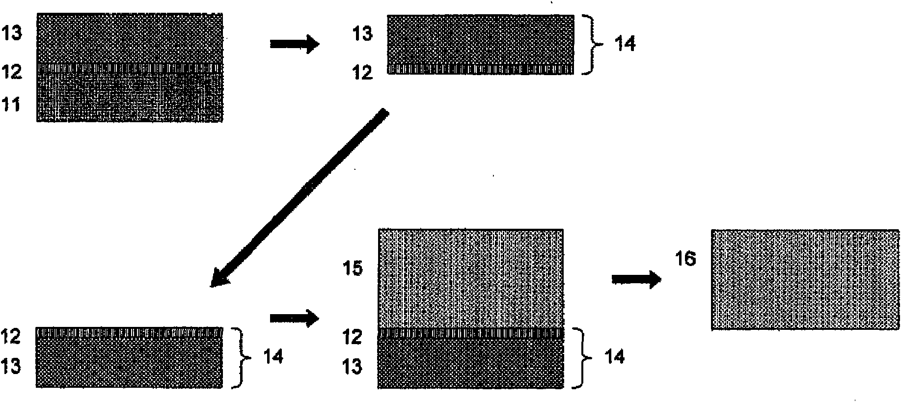
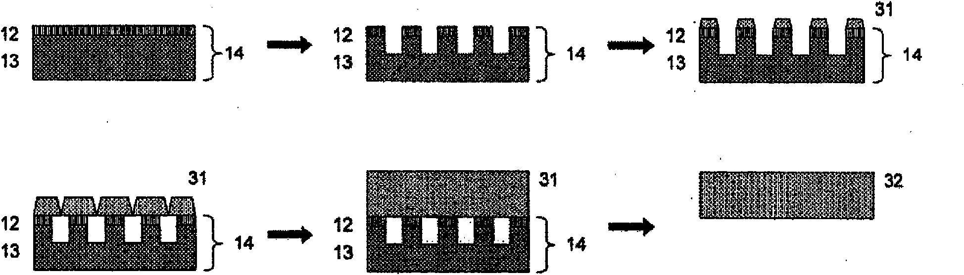
Examples
Embodiment 1
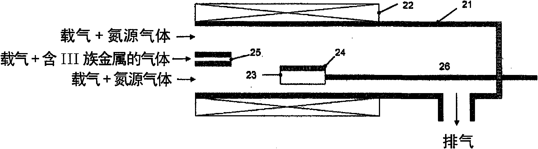
[0109] This is an example in which a substrate for self-supporting substrate production was produced using the HVPE method as a vapor deposition method. In this embodiment, a (111) silicon single crystal substrate with a diameter of 2 inches and a thickness of 280 μm was used as the base substrate, and aluminum nitride was used as the material of the single crystal layer and the non-single crystal layer.
[0110] figure 2 The HVPE apparatus shown is equipped with the reactor main body which consists of the cylindrical quartz glass reaction tube 21, the external heating unit 22 arrange|positioned outside this reaction tube 21, and the support stand 23 arrange|positioned inside this reaction tube. Furthermore, it is a structure in which the carrier gas and the raw material gas are supplied from one end portion of the reaction tube 21, and the carrier gas and the unreacted reaction gas are discharged from the opening provided in the side wall near the other end portion. In addi...
Embodiment 2
[0122] In this example, the apparatus and substrate described in Example 1 were used, and in addition to the flow of Example 1, a single crystal layer was formed on the base substrate, and the supply of aluminum trichloride as a raw material gas was interrupted, and then an additional supply of 10 A process in which 0.1 sccm of oxygen per second is used as an oxygen-containing gas. The deposition conditions of the single crystal layer and the polycrystalline layer, and the peeling conditions of the silicon substrate were the same, and a substrate for self-supporting substrate production having a thickness comparable to that of Example 1 was obtained.
[0123] The θ-2θ measurement of X-ray diffraction was performed from the exposed side of the polycrystalline layer of the substrate for self-supporting substrate production, and the intensity ratio was I (002) / I (100) is 1.5. In addition, the surface on the exposed side of the single crystal layer was the same mirror surface a...
Embodiment 3
[0126] In this example, the same apparatus and substrate as in Example 1 were used to form an amorphous layer as the non-single crystal layer in Example 1. The first layer was deposited on the silicon substrate as the base substrate under the same raw material supply conditions as in Example 1 for 2 minutes to form a 0.2 μm single crystal layer. Next, the supply of aluminum trichloride was stopped, and the pressure was changed to 500 Torr. The temperature of the reaction tube was maintained at 500°C by the external heating unit, while the power supply to the support table was removed, and the temperature of the base substrate was set to 800°C. These operations were performed within 10 minutes after the supply of aluminum trichloride was temporarily stopped. Next, the supply of aluminum trichloride gas was turned on again, and maintained for 240 minutes, to further deposit an aluminum nitride amorphous layer of 220 μm. The silicon substrate was removed by chemical etching to ...
PUM
| Property | Measurement | Unit |
|---|---|---|
| thickness | aaaaa | aaaaa |
| thickness | aaaaa | aaaaa |
| thickness | aaaaa | aaaaa |
Abstract
Description
Claims
Application Information
 - R&D
- Intellectual Property
- Life Sciences
- Materials
- Tech Scout
- Unparalleled Data Quality
- Higher Quality Content
- 60% Fewer Hallucinations
Browse by: Latest US Patents, China's latest patents, Technical Efficacy Thesaurus, Application Domain, Technology Topic, Popular Technical Reports.
© 2025 PatSnap. All rights reserved.Legal|Privacy policy|Modern Slavery Act Transparency Statement|Sitemap|About US| Contact US: help@patsnap.com