
Double-junction solar cell of broad spectrum photovoltaic effect and preparation method thereof

A technology of solar cells and broad-spectrum light, applied in the field of Si optoelectronic materials, can solve the problem of inability to fully utilize the energy of a single photon, and achieve the effect of broadening the photovoltaic effect spectrum and improving cell efficiency

Inactive Publication Date: 2011-02-02
INST OF SEMICONDUCTORS - CHINESE ACAD OF SCI
View PDF8 Cites 7 Cited by
  • Summary
  • Abstract
  • Description
  • Claims
  • Application Information

AI Technical Summary

Problems solved by technology

Crystalline silicon solar cells have very high quantum efficiency in the 600-900nm band, but above 1100nm, they cannot absorb due to the band gap, and below 300nm, they cannot fully utilize the energy of a single photon.

Method used


Image

  • Double-junction solar cell of broad spectrum photovoltaic effect and preparation method thereof
  • Double-junction solar cell of broad spectrum photovoltaic effect and preparation method thereof
  • Double-junction solar cell of broad spectrum photovoltaic effect and preparation method thereof

Examples


Embodiment example

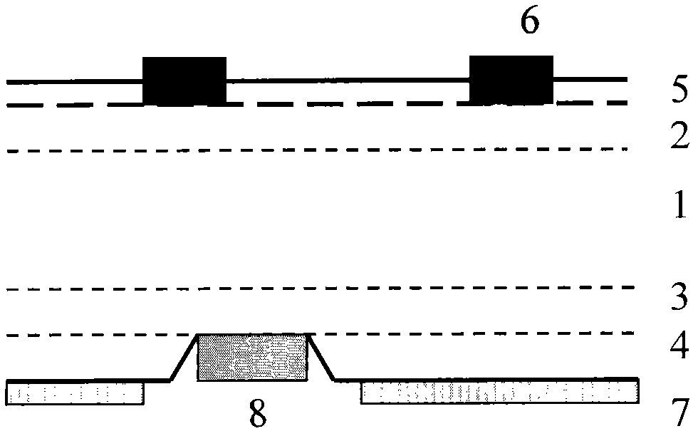
[0108] This embodiment is based on image 3 The method for preparing a crystalline silicon double-junction solar cell with a wide-spectrum photovoltaic effect is realized, and the specific process is as follows:

[0109]The wide-spectrum anti-reflection structure is prepared on the light-facing surface of the first conductivity type Si substrate 1, which is to scan and irradiate the Si surface with an ultrashort pulse laser in an atmosphere of sulfur S, selenium Se, and tellurium Te elements, and the pulse width is less than 100 pico. seconds, the pulse frequency is less than 5kHz, and the energy density is about 1-10kJ / m 2 , so that the Si surface forms a micron-scale crystal cone morphology, so as to achieve the purpose of broad-spectrum anti-reflection incident light. Using NaOH and C 2 h 5 The OH mixed alkaline solvent corrodes the Si surface, and because it has different corrosion rates for each (hkl) crystal plane of Si, a pyramidal surface structure can be formed;

...


PUM


Abstract

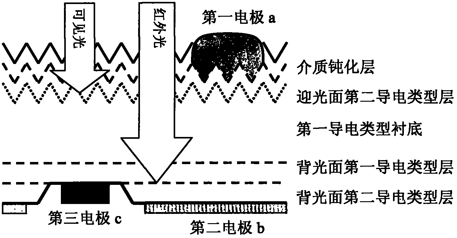
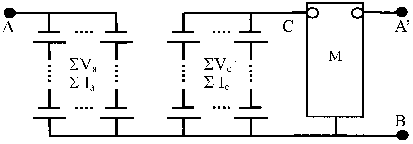
The invention discloses a double-junction solar cell of broad spectrum photovoltaic effect and a preparation method thereof. The cell is provided with a light-facing surface second conductive type layer and a medium passivation layer in turn on the light-facing surface of a first conductive type substrate, wherein the surface of the medium passivation layer has a broad spectrum anti-reflection structure; the cell is provided with a backlight surface first conductive type layer and a backlight surface second conductive type layer in turn on the backlight surface of the first conductive type substrate; a first electrode formed on the light-facing surface second conductive type layer, a second electrode formed on the backlight surface second conductive type layer and a third electrode formed on the backlight surface first conductive type layer form the backlight surface first conductive type layer; and the same electrodes of the adjacent cells are interconnected to adjust the voltage and connected in parallel to form two-end output of a cell panel assembly. By using the double-junction solar cell, the photoelectric conversion spectrum of the cell is broadened so that the efficiency of the cell is improved.

Description

technical field [0001] The invention relates to the technical field of Si optoelectronic materials, in particular to a double-junction solar cell with wide-spectrum photovoltaic effect and a preparation method thereof. Background technique [0002] Silicon solar cells are the main body in today's photovoltaic market, and crystalline silicon solar cells have the highest conversion efficiency, with a world record of 24.7%. Crystalline silicon solar cells have very high quantum efficiency in the 600-900nm band, but above 1100nm cannot absorb due to the band gap, and below 300nm cannot fully utilize the energy of a single photon. Therefore, in order to continue to improve the efficiency of crystalline silicon solar cells, it is necessary to work hard on long-wave and short-wave bands. [0003] Multi-level light absorption is a broad-spectrum light absorption method [1] , Whether multi-level light absorption can be achieved in Si materials has always been of great interest to t...

Claims


Application Information

Patent Timeline
Patent Type & Authority Applications(China)
IPC IPC(8): H01L31/05H01L31/0352H01L31/0304
CPCY02E10/50
Inventor 韩培德
Owner INST OF SEMICONDUCTORS - CHINESE ACAD OF SCI
Learn More