Black silicon methyl sulfonyl methane (MSM) structure photoelectric detector and preparation method thereof

A technology of photodetector and black silicon, which is applied in the field of photodetector, can solve the problem of low sensitivity and achieve the effect of high responsivity and wide spectral response range

Inactive Publication Date: 2011-02-09
UNIV OF ELECTRONIC SCI & TECH OF CHINA
View PDF3 Cites 19 Cited by
  • Summary
  • Abstract
  • Description
  • Claims
  • Application Information

AI Technical Summary

Problems solved by technology

Therefore, low sensitivity is still a key pr

Method used


Image

  • Black silicon methyl sulfonyl methane (MSM) structure photoelectric detector and preparation method thereof
  • Black silicon methyl sulfonyl methane (MSM) structure photoelectric detector and preparation method thereof
  • Black silicon methyl sulfonyl methane (MSM) structure photoelectric detector and preparation method thereof

Examples


preparation example Construction

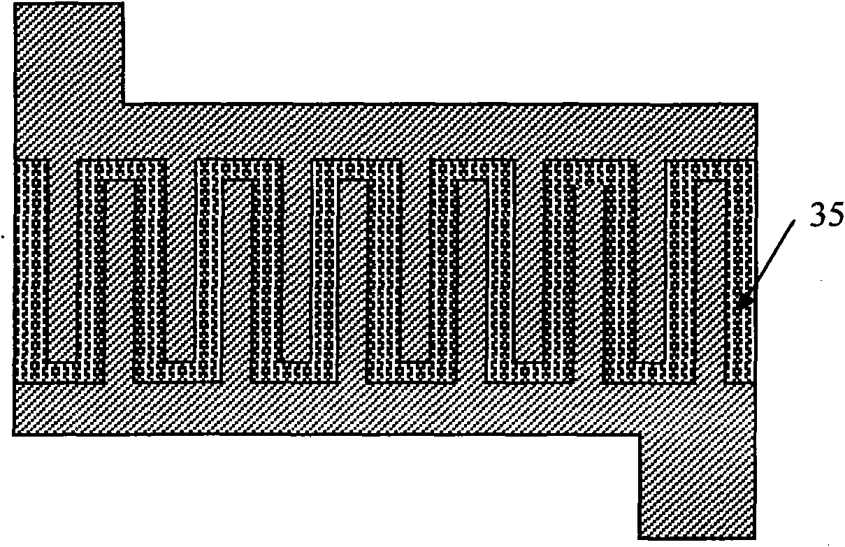
[0031] The preparation method includes the following steps: ①Preparing a black silicon thin film layer: implanting doping materials on a single crystal silicon substrate by ion implantation to prepare a surface microstructure; ②Spin-coating a layer of photoresist on the surface of the black silicon thin film layer , and use a specific interdigitated electrode mask pattern to pattern the photoresist; ③ immerse the patterned substrate in an alkali etching solution to etch, and remove the unprotected black silicon film layer on the pattern; ⑤ Deposition barrier ④ using the overlay process to prepare the interdigitated electrode pattern again; ⑥ then deposit the electrode material layer and pattern it into the shape of the interdigitated electrode; ⑦ deposit the passivation layer; ~40 minutes.

[0032] The doping material for ion implantation in step ① is S or Se or Te, and the doping concentration range is 1×10 14 and 5×10 15 ion / cm 2 between.

[0033] The preparation of the ...

Embodiment 1

[0038] The specific implementation steps are as follows:

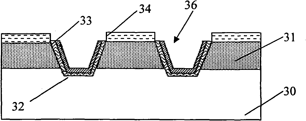
[0039] 1. Prepare the black silicon material 31, the thickness of the obtained black silicon layer is 1-10 μm.

[0040] 2. Spin-coat a layer of photoresist on the surface of the black silicon material, and pattern the photoresist with a specific interdigitated electrode mask pattern.

[0041] 3. Immerse the patterned substrate in the alkaline etching solution for a specific period of time to remove the unprotected black silicon layer on the pattern.

[0042] 4. Corrosion in a specific concentration of KOH solution to form a U-shaped structure 36, and the depth of the U-shaped groove is 3-10 μm.

[0043] 5 Prepare the interdigitated electrode pattern above the U-shaped groove by using the overlay process;

[0044] 6. Deposit a thin a-Si:H barrier layer 32 with a thickness of about 30-100 nm.

[0045] 7. Deposit a metal Al or ITO thin film with a thickness of about 50-100 nm as the interdigital electrode material 33, ...

Embodiment 2

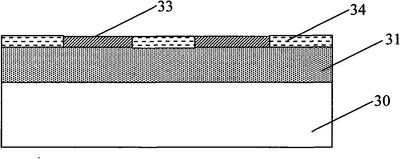
[0050] The difference between this implementation example and implementation example 1 is that step 3, step 4 and step 5 are cancelled, and the rest are the same as example 1.

[0051] The resulting device structure is as image 3 shown.


PUM

PropertyMeasurementUnit
Thicknessaaaaaaaaaa
Thicknessaaaaaaaaaa
Thicknessaaaaaaaaaa

Abstract

The invention discloses a black silicon methyl sulfonyl methane (MSM) structure photoelectric detector, which comprises a monocrystalline silicon substrate and is characterized in that: the surface of the monocrystalline silicon substrate is provided with a black silicon thin film layer serving as a photosensitive area; an interdigital electrode is arranged on the black silicon thin film layer; a barrier layer is arranged below the interdigital electrode; and a passive layer is arranged in the area besides the area where the interdigital electrode is arranged. The detector has a wide spectral response range and high responsiveness, and can be used for detecting ultraviolet light, visible light or near infrared light.

Description

technical field [0001] The invention relates to the technical field of photodetectors, in particular to a black silicon MSM photodetector and a preparation method thereof. Background technique [0002] Silicon is an important semiconductor material, and it is also the main material of the current microelectronic integrated circuit technology, and plays an extremely important role in VLSI. If silicon is used as the basic material and mature standard integrated circuit technology is used to fabricate optoelectronic devices and optoelectronic integrated circuits, it will have great advantages over other compound optoelectronic devices. However, there is still no major breakthrough in the research of silicon-based photodetector devices. sexual progress. When the light wave is incident on the surface of the silicon photoelectric device, about 30% of the light energy is reflected, so the responsivity of the silicon MSM-PD is only about 0.2A / W, and the quantum efficiency is also v...

Claims


Application Information

Patent Timeline
IPC IPC(8): H01L31/0248H01L31/101H01L31/18
CPCY02P70/50
Inventor 蒋亚东赵国栋吴志明李伟姜晶张安元郭正宇
Owner UNIV OF ELECTRONIC SCI & TECH OF CHINA
Why Eureka
Try Eureka