Method for enhancing radiation resistant characteristic of LDMOS (Laterally Diffused Metal Oxide Semiconductor)

An anti-radiation and characteristic technology, which is applied in the manufacture of electrical components, circuits, semiconductors/solid-state devices, etc., can solve problems that affect the reliability of devices and circuits, increase electric fields, and reduce breakdown voltage of devices, so as to improve anti-radiation ability, improve radiation resistance, and reduce the effect of reinforcement costs

Inactive Publication Date: 2011-02-16
PEKING UNIV
View PDF2 Cites 2 Cited by
  • Summary
  • Abstract
  • Description
  • Claims
  • Application Information

AI Technical Summary

Problems solved by technology

However, since the structure introduces the STI dielectric region in the drift region, holes will be trapped after being irradiated, which increases the electric field, reduces the breakdown voltage of the device, and leads to performance degradation, which seriously affects the performance of the device and the circuit. Reliability under space radiation environment

Method used


Image

  • Method for enhancing radiation resistant characteristic of LDMOS (Laterally Diffused Metal Oxide Semiconductor)
  • Method for enhancing radiation resistant characteristic of LDMOS (Laterally Diffused Metal Oxide Semiconductor)
  • Method for enhancing radiation resistant characteristic of LDMOS (Laterally Diffused Metal Oxide Semiconductor)

Examples


Embodiment Construction

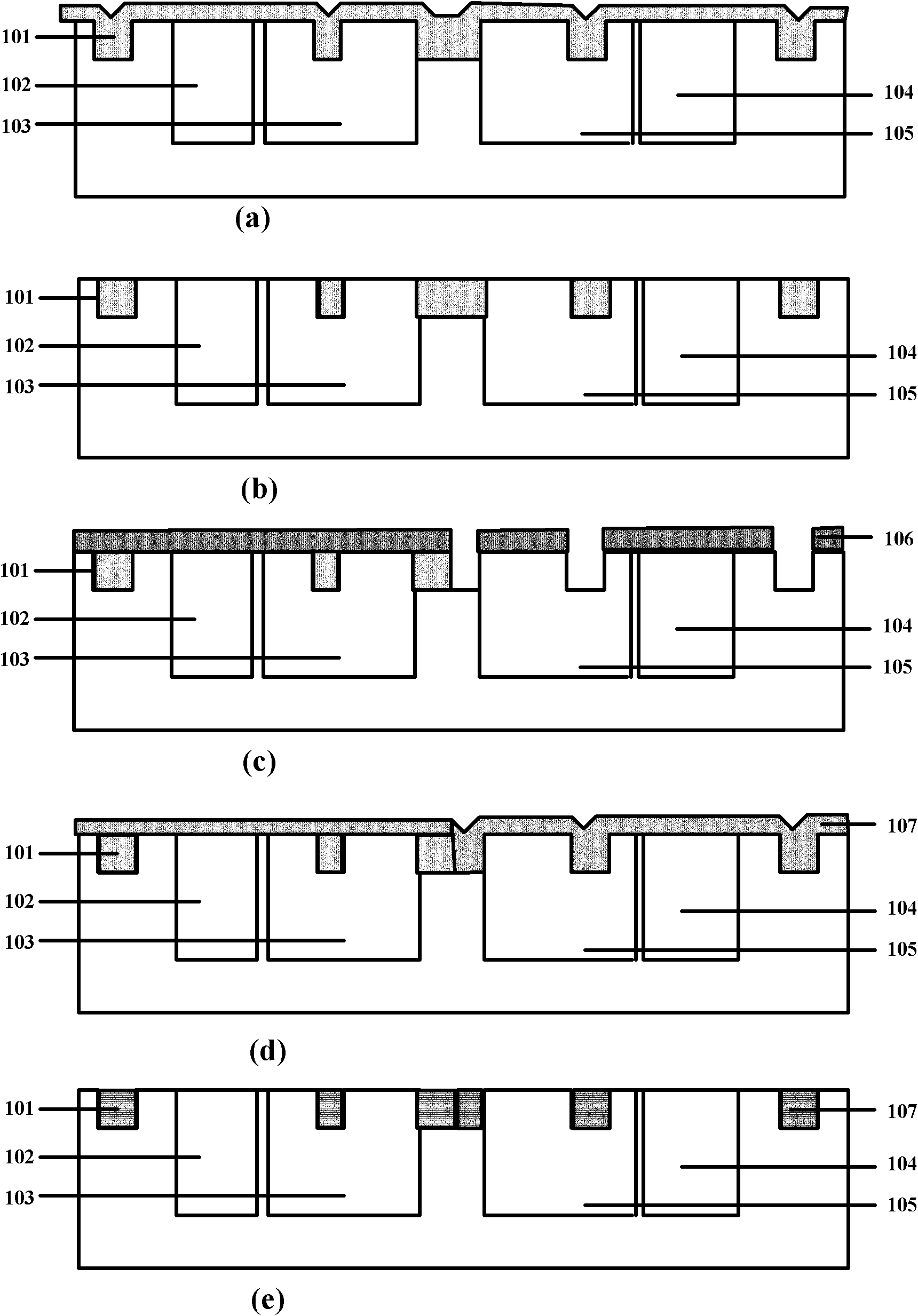
[0017] In the preparation of the integrated circuit of the present invention, the materials used to form the trench isolation region and the drift region dielectric layer of the N-type and P-type LDMOS devices are different, so the process steps for the preparation of the N-type and P-type LDMOS transistor isolation regions and the drift region are separated. , the process is as follows:

[0018] image 3 (a)-(e) are the process flow and the cross-sectional schematic diagrams corresponding to each step of the method for preparing the isolation region and the drift region of the N-type and P-type LDMOS devices of the present invention.

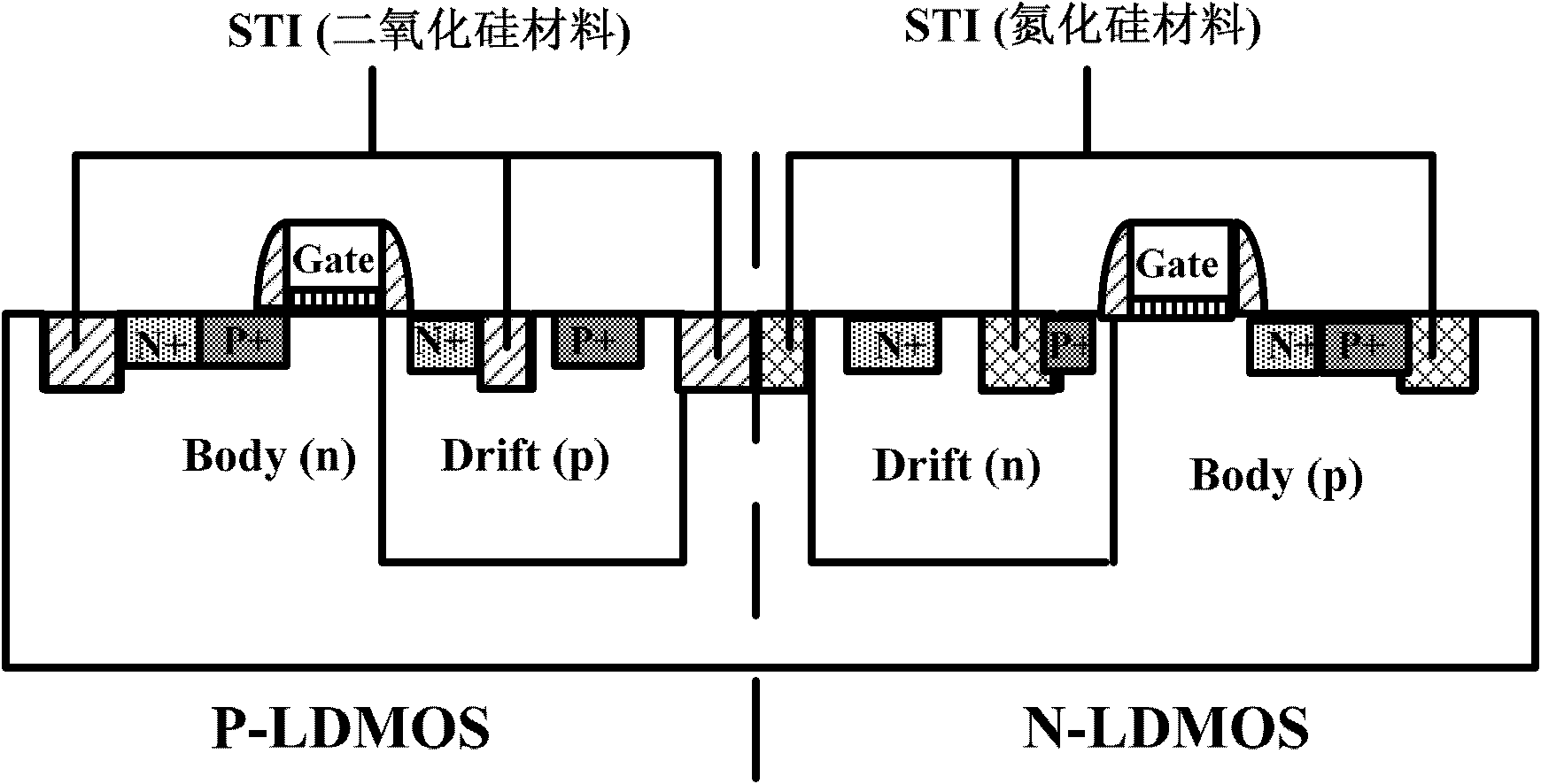
[0019] 101---deposited silicon dioxide; 102---N well body region of P-type LDMOS transistor; 103---P well drift region of P-type LDMOS transistor; 104---P well of N-type LDMOS transistor Body region; 105---N well drift region of N-type LDMOS transistor; 106---photoresist; 107---nitride medium.

[0020] The specific process of the dielectric l...


PUM


Abstract

The invention provides a method for enhancing the radiation resistant characteristic of an LDMOS (Laterally Diffused Metal Oxide Semiconductor), belonging to the technical field of radiation resistance of an integrated circuit and aiming at the conventional LDMOS transistor structure of a radio-frequency power device. The method is characterized in that materials selected by and used for a drift region STI dielectric layer and a device isolation region dielectric layer of an N type LDMOS transistor are different from the materials selected by and used for a drift region STI dielectric layer and a device isolation region dielectric layer of a P type LDMOS transistor; the drift region STI dielectric layer and a device isolation region of the N type LDMOS transistor select and use the materials which are easier to trap electrons after being radiated; and the filling materials of the drift region STI dielectric layer and the device isolation region dielectric layer of the P type LDMOS transistor are materials which are easier to trap cavities. The invention is used for the radiation resistant design of a semiconductor device and the integrated circuit and can enhance the radiation resistant capability of the integrated circuit and reduce the strengthening cost.

Description

technical field [0001] The invention relates to integrated circuit anti-irradiation technology, in particular to a method for improving the anti-irradiation performance of power device LDMOS. Background technique [0002] With the development of radio frequency integrated circuits and the continuous increase of the wireless communication market, more and more attention has been paid to radio frequency power devices in wireless communication such as personal / family wireless communication equipment, mobile communication equipment and even military radar. getting bigger. In the transceiver system of the radio frequency circuit, the power amplifier is a very important part. Power amplifiers are usually required to process large signals and require good stability, which requires the core power components of the circuit to have good high voltage resistance and reliability. The lateral double-diffused LDMOS transistor based on silicon material has the advantages of high breakdown...

Claims


Application Information

Patent Timeline
Patent Type & Authority Applications(China)
IPC IPC(8): H01L21/762
Inventor 薛守斌杨东黄如张兴
Owner PEKING UNIV
Why Eureka
Try Eureka