GaN light-emitting diodes with low-temperature p-type GaN layer

A technology based on light-emitting diodes and gallium nitride, which is applied in the direction of electrical components, circuits, semiconductor devices, etc., can solve problems such as structural damage, the influence of light-emitting diodes, and the influence of device luminous intensity, and achieve the improvement of reverse breakdown voltage and luminous intensity. Improved effect

Inactive Publication Date: 2011-04-06
上海蓝宝光电材料有限公司
View PDF1 Cites 18 Cited by
  • Summary
  • Abstract
  • Description
  • Claims
  • Application Information

AI Technical Summary

Problems solved by technology

On the one hand, the compressive stress caused by lattice mismatch will form a large compressive strain electric field (ie, piezoelectric field effect) effect)), and the existence of the piezoelectric field effect will make the wave functions of electrons and holes separated in space, thus causing the weakening of the radiative recombination intensity
In addition, the mechanical stress caused by the above-mentioned compressive strain will further deteriorate the quality of the epitaxial layer, thereby affecting the luminous intensity of the device
Secondly, the p-type AlGaN electron blocking layer must be grown above 1000°C to obtain better crystal quality, while the growth temperature of the InGaN / GaN MQW active layer is 700°C to 850°C, so when InGaN / GaN MQW When the temperature rises above 1000°C after the growth of the active layer, the structure of the InGaN / GaN multi-quantum well active layer grown at low temperature will be destroyed, thus affecting the luminous efficiency of the light-emitting diode
Thirdly, since the growth temperature of the p-type AlGaN electron blocking layer is relatively high, and the diffusion coefficient of the p-type dopant (such as Mg) increases rapidly at high temperature, during the high-temperature growth of the p-type AlGaN electron blocking layer, the p Type dopants will inevitably diffuse into the underlying InGaN / GaN multi-quantum well active region, which will have a serious impact on light-emitting diodes

Method used


Image

  • GaN light-emitting diodes with low-temperature p-type GaN layer
  • GaN light-emitting diodes with low-temperature p-type GaN layer
  • GaN light-emitting diodes with low-temperature p-type GaN layer

Examples


Embodiment 1

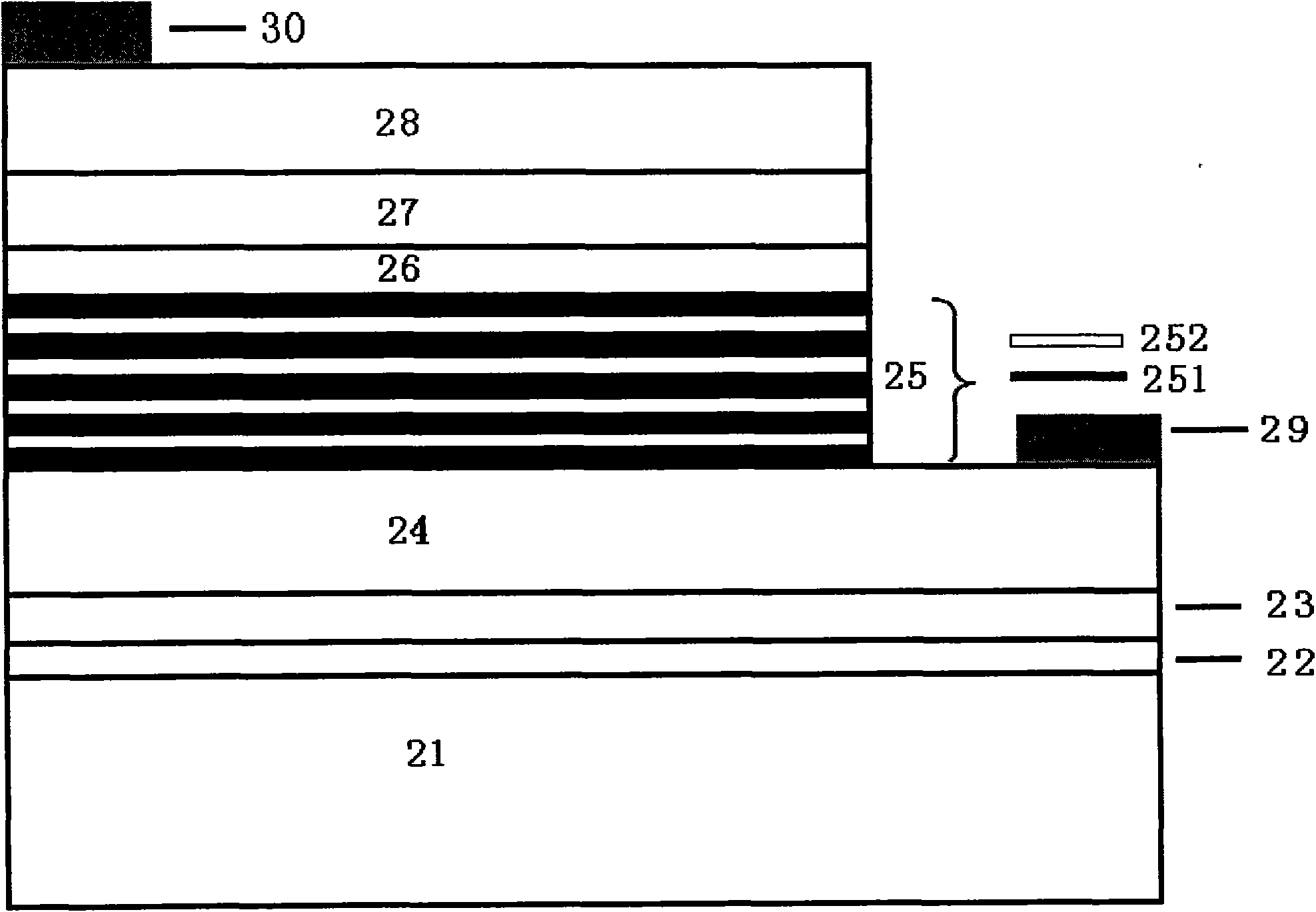
[0066] figure 2 Shown is a GaN-based light-emitting diode with a low-temperature p-type GaN insertion layer according to the present invention. It is manufactured under the same process conditions as Comparative Example 1, except that a low-temperature p-type nitride layer with a thickness of 20-100 nanometers is inserted between the InGaN / GaN multi-quantum well active light-emitting layer 25 and the p-type AlGaN electron blocking layer 27. Gallium insertion layer 26 , and the lower surface of the low-temperature p-type GaN insertion layer 26 is in contact with the GaN thin layer in the multi-quantum well active light-emitting layer 25 . The doping concentration of magnesocene in the low-temperature p-type gallium nitride layer is 10 19 ~10 21 cm -3 .

[0067] The specific growth conditions of the low-temperature p-type GaN insertion layer 26 are as follows: reaction temperature 600-900°C, reaction chamber pressure 200-500 Torr, carrier gas flow rate 5-20 liters / min, ammo...


PUM


Abstract

The invention relates to GaN light-emitting diodes with a low-temperature p-type GaN layer. The main difference between the structure of the GaN light-emitting diodes of the invention and the structure of the existing GaN light-emitting diodes is that a low-temperature p-type GaN layer grows between an InGaN/GaN multiple-quantum well active light-emitting layer and a p-type AlGaN electron blocking layer, thereby physically separating the InGaN/GaN multiple-quantum well active light-emitting layer from the p-type AlGaN electron blocking layer on an interface. Results show that the luminous intensity and reverse breakdown voltage of the GaN light-emitting diodes are greatly improved.

Description

technical field [0001] The invention relates to a gallium nitride (GaN) light-emitting diode, in particular to a gallium nitride light-emitting diode with a low-temperature p-type GaN layer. Background technique [0002] At present, III-V semiconductor optoelectronic materials are known as the third generation semiconductor materials. GaN-based light-emitting diodes have become the focus of industry research because they can produce light-emitting diodes (referred to as "LEDs") of various colors (especially blue or violet light that requires a high energy gap) by controlling the composition of materials. [0003] The epitaxial growth of GaN-based semiconductor materials or devices currently mainly adopts MOCVD technology. In the process of growing nitride semiconductors (GaN, AlN, InN and their alloy nitrides) using MOCVD technology, sapphire is usually used as the substrate for heteroepitaxy because there is no substrate material that matches the GaN lattice. However, the...

Claims


Application Information

Patent Timeline
Patent Type & Authority Applications(China)
IPC IPC(8): H01L33/00
Inventor 马平丁成刘慰华李刚
Owner 上海蓝宝光电材料有限公司
Why Eureka
Try Eureka